1-Aug-2012
The PCB design guidelines outlined in Zynq datasheet must be followed for trace matching, etc.
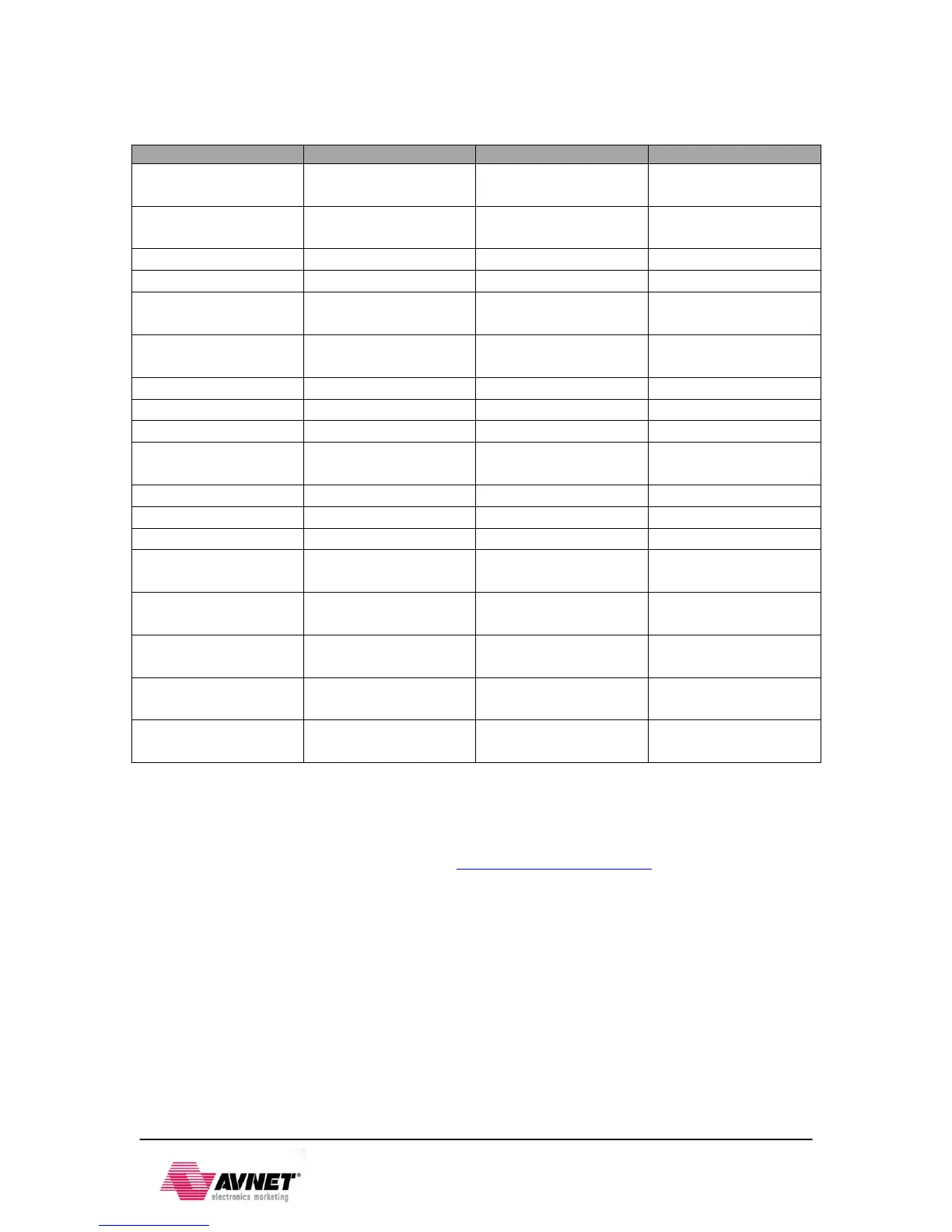
Table 1 - DDR3 Connections
Differential clock
output
Differential clock
output
RAS column address
select
Output dynamic
termination
I/O Differential data
strobe
I/O Differential data
strobe
I/O Used to calibrate
input termination
I/O Used to calibrate
input termination
For best DDR3 performance, DRAM training is enabled for write leveling, read gate, and read
data eye options in the PS Configuration Tool in Xilinx Platform Studio (XPS). The PS
Configuration tools’ Memory Configuration Wizard contains two entries to allow for DQS to Clock
Delay and Board Delay information to be specified for each of the four byte lanes. These
parameters are specific to every PCB design. Xilinx Answer Record 46778 provides a tool for
calculating these parameters by a printed circuit board design engineers. The Excel worksheet
file ar46778_board_delay_calc.xlsx included in the answer record provides instructions in the
worksheet for calculating these board training details based upon specific trace lengths for certain
DDR3 signals. Using the information from the trace length reports pertaining to the DDR3
interface for ZedBoard these delay values can be recreated by following the directions found in
the Excel worksheet.
The PCB lengths are contained in the ZedBoard PCB trace length reports. The DQS to CLK
Delay and Board Delay values are calculated specific to the ZedBoard memory interface PCB
design. The AR46778 worksheet allows for up to 4 memory devices to be configured for DDR3
4x8 flyby topology. Note that ZedBoard is configured for DDR3 2x16 flyby routing topology. The
first two clock trace midpoint values (CLK0 and CLK1) are used to represent the Micron device
electrically nearest to 7Z020 (IC26) and the second two clock trace midpoint values (CLK2 and