12
3.7 VR Calibration and Switch Setting Procedure
3.7.1 VR/Switch Function Explanation
3.7.1.1 VR Function Explanation
VR
Adjustment
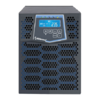
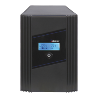
MS1K(R)/2K(R)/3K(R)
A. Logic Board: MS-I9919-x
O/P Voltage Balance VR1
Output Voltage Selection SW1
CPU Reset SW2
B. Driver Board: MSD9917-x or MSADxxx for 1K; MSD9910-x or
MSBDxxx for 2K; MSCDxxx for MS3K
Charger Output Voltage VR1
3.7.2. Setting Procedure
3.7.2.1. Equipment Installation
Please connect the equipment mentioned in 3.2. as the drawing
Shown in the below:
I/P
BATT
O/P
POWER
METER
RES
LOAD
DC
SOURCE
AC
SOURCE
METER
METER
 Loading...