107
Chapter 5 Theory of Operation
Main Output Circuitry
4
5
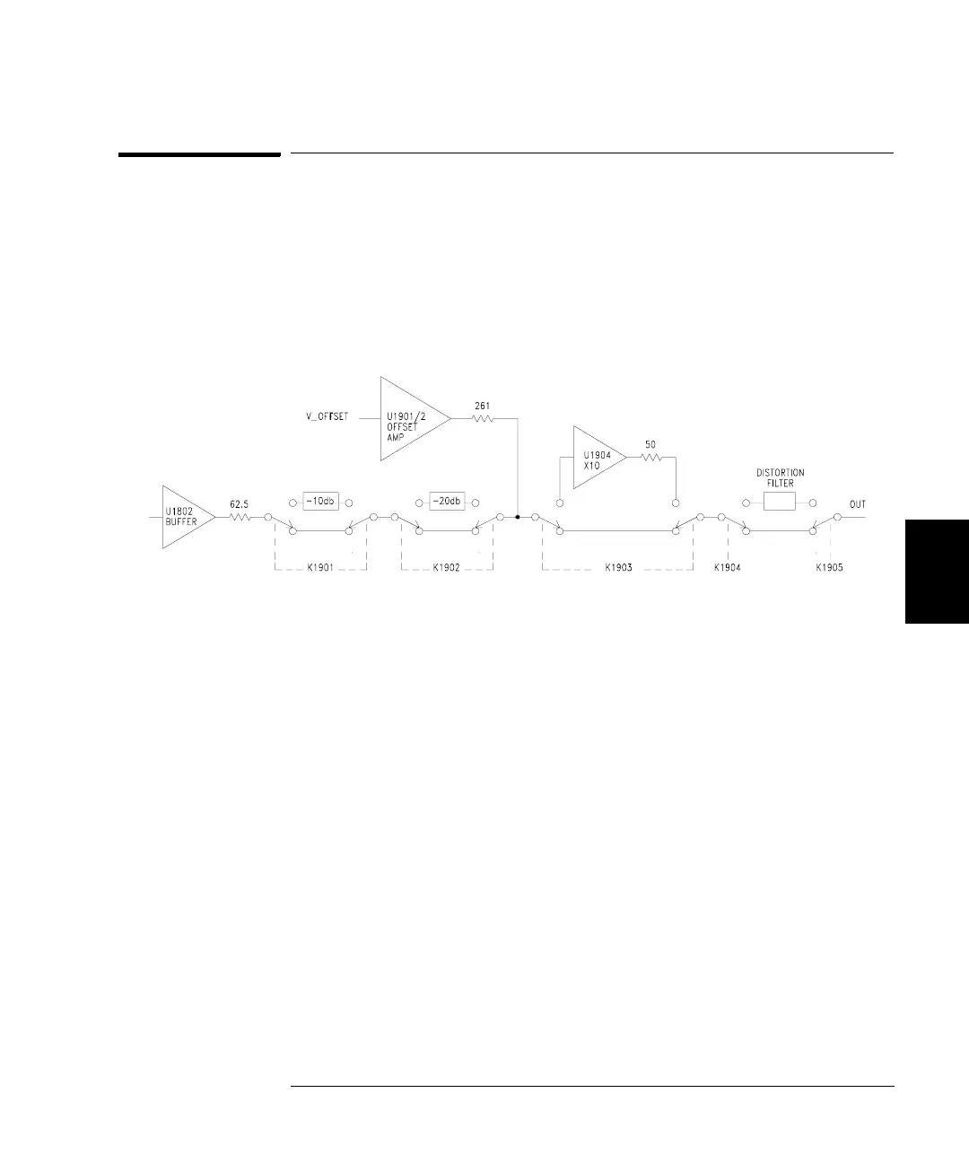
Main Output Circuitry
See “A1 Main Output Circuitry Schematic” on page 203.
The main output circuitry attenuates or amplifies the waveform to its
final amplitude level and adds any dc offset required. The output is
also protected against harmful combinations of load impedance and
output voltage.
R1915, R1917, and R1918 form a –10 dB attenuator that is switched
by K1901. Similarly, R1916, R1919, R1920, and R1921 form a 20 dB
attenuator that is switched by K1902. U1903, U1904, and the associated
components form a 20 dB amplifier that is switched by K1903. K1901
through K1903 are latching relays controlled by signals from U305.
0 dB path is shown
 Loading...