5-14 Service Guide E8364-90026
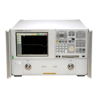
Theory of Operation PNA Series Microwave Network Analyzers
Source Group Operation E8362B, E8363B, E8364B
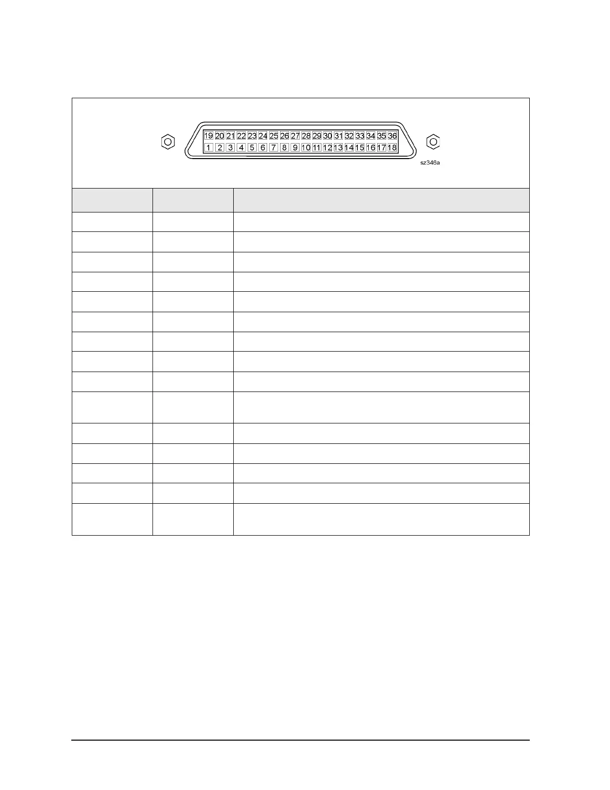
Table 5-4 HANDLER I/O Connector Key Pin Assignments
Rectangular 36-Pin Female Connector
Pin Numbers Name Function
1 GND 0 V, ground reference
2 INPUT1 TTL in, negative pulse (1 μs min) latches OUTPUT1-2
3–4 OUTPUT1–2 TTL out, latched
5–12 Port A0–7 Out TTL out, latched
13–20 Port B0–7 Out TTL out, latched
21–24 Port C I/O TTL I/O, latched
25–28 Port D I/O TTL I/O, latched
29 Port C Status TTL out, low = input mode, high = output mode
30 Port D Status TTL out, low = input mode, high = output mode
31 Output Strobe
Write Strobe
TTL out, active low data write strobe (1 μs min)
32 No connect Not used
33 Pass Fail TTL out, latched, indicates pass fail (programmable polarity)
34 +5 V +5 Vdc, 100 mA max.
35 Sweep End TTL out, active low (10 μs min) indicates sweep done
36 Pass/Fail
Write Strobe
TTL out, active low pass/fail write strobe (1 μs min)
 Loading...