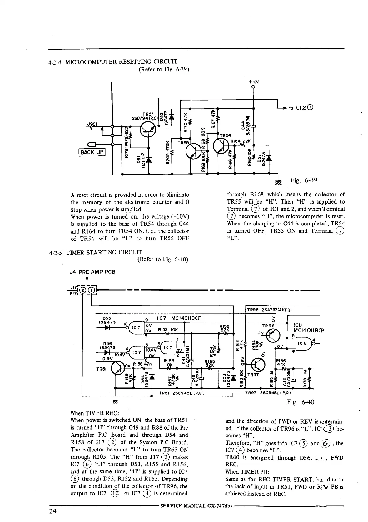
4-2-4 MICROCOMPUTER RESETTING CIRCUIT
(Refer
to
Fig. 6-39)
TR!57
N~
2SD794(P,O)
:g~
J901
~
I BACK
UPI
A reset circuit
is
provided in order to eliminate
the memory
of
the electronic counter and 0
Stop when power
is
supplied.
When
power
is
turned on, the voltage (+l0V)
is
supplied to the base
of
TR54 through C44
and
Rl64
to
tum
TR54
ON,
i.e.,
the collector
of
TR54 will be
"L"
to
tum
TR55 OFF
4-2-5 TIMER STARTING CIRCUIT
(Refer
to
Fig. 6-40)
J4
PRE
AMP
PCB
t
IC?
MCl4011BCP
Rl53
IOK
3
IC7
OV
:I!
2
-~
.,.,
UN
.,;
!I!
a:
..,:.:
..,o
_,._
a::"'
Rl5!5
82K
TR!51
2SC94!5L ( P,O)
When
TIMER REC:
When
power
is
switched
ON,
the base
of
TR5 l
is
turned
"H''
through C49 and R88
of
the Pre
Amplifier P.C Board and through D54 and
R158
of
J17 @
of
the Syscon
P.C
Board.
The collector becomes
"L"
to
tum
TR63
ON
throu~
R205. The
"H"
from
J1
7 @ makes
IC7
~
"H"
through D53,
Rl
55 and R1·56,
and at the same time,
"H"
is
supplied
to
IC7
@ through D53, R152 and
Rl53.
Depending
on the condition
of
the collector
of
TR96, the
output to IC7
@ or IC7 @
is
determined
+1ov
to
1c1,2(V
Fig. 6-39
through
Rl
68 which means the collector
of
TR5 5 will
be
"H". Then
"H"
is supplied to
Terminal (j)
of
ICl and 2, and when Terminal
(j) becomes
"H",
the microcomputer is reset.
When
the charging
to
C44
is
completed, TR54
is
turned OFF, TR55
ON
and Tenninal (j)
"L".
TR96
2SA7331AHPO)
Rl52
82K
"'
!
!
,,,,._
..,..,
ON
a,
0N
..,
.....
"'
!!?
u"!
iE
"'
TR97
2SC94!5L ( P,Q)
Fig.
6-40
and the direction
of
FWD
or REV
is
de-termin-
ed. If the collector
of
TR96
is
"L",
IC)
G)
be-
comes "H".
Therefore,
"H"
goes into IC7
(})
and(§)
, the
IC7
@ becomes
"L".
TR60
is
energized through D56, i. e.,,
FWD
REC.
When
TIMER PB:
Same
as
for REC TIMER START,
but
due to
the lack
of
input in TR51,
FWD
or
REV
PB
is
achieved instead
of
REC.
----------------
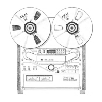
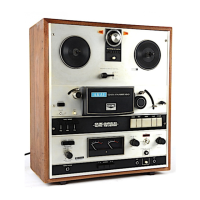
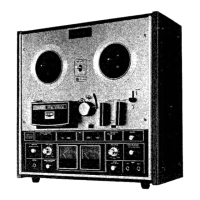
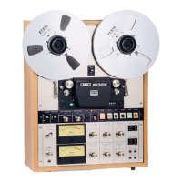
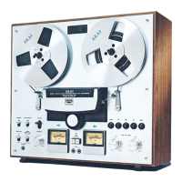
SERVICE MANUAL GX-747dbx
----------------
24
 Loading...