EasyManua.ls Logo

Alinx AXU2CGA - Part 5: Emmc Flash (Only for AXU2 CGB)

Alinx AXU2CGA
29 pages
Print Icon
To Next Page IconTo Next Page
To Previous Page IconTo Previous Page
Loading...
ZYNQ Ultrascale + FPGA Board AXU2CGA/B User Manual
12 / 29
Amazon Store: https://www.amazon.com/alinx
MIO2_QSPI0_IO2
PS_MIO2_500
AF15
MIO3_QSPI0_IO3
PS_MIO3_500
AH15
MIO4_QSPI0_IO0
PS_MIO4_500
AH16
MIO5_QSPI0_SS_B
PS_MIO5_500
AD16
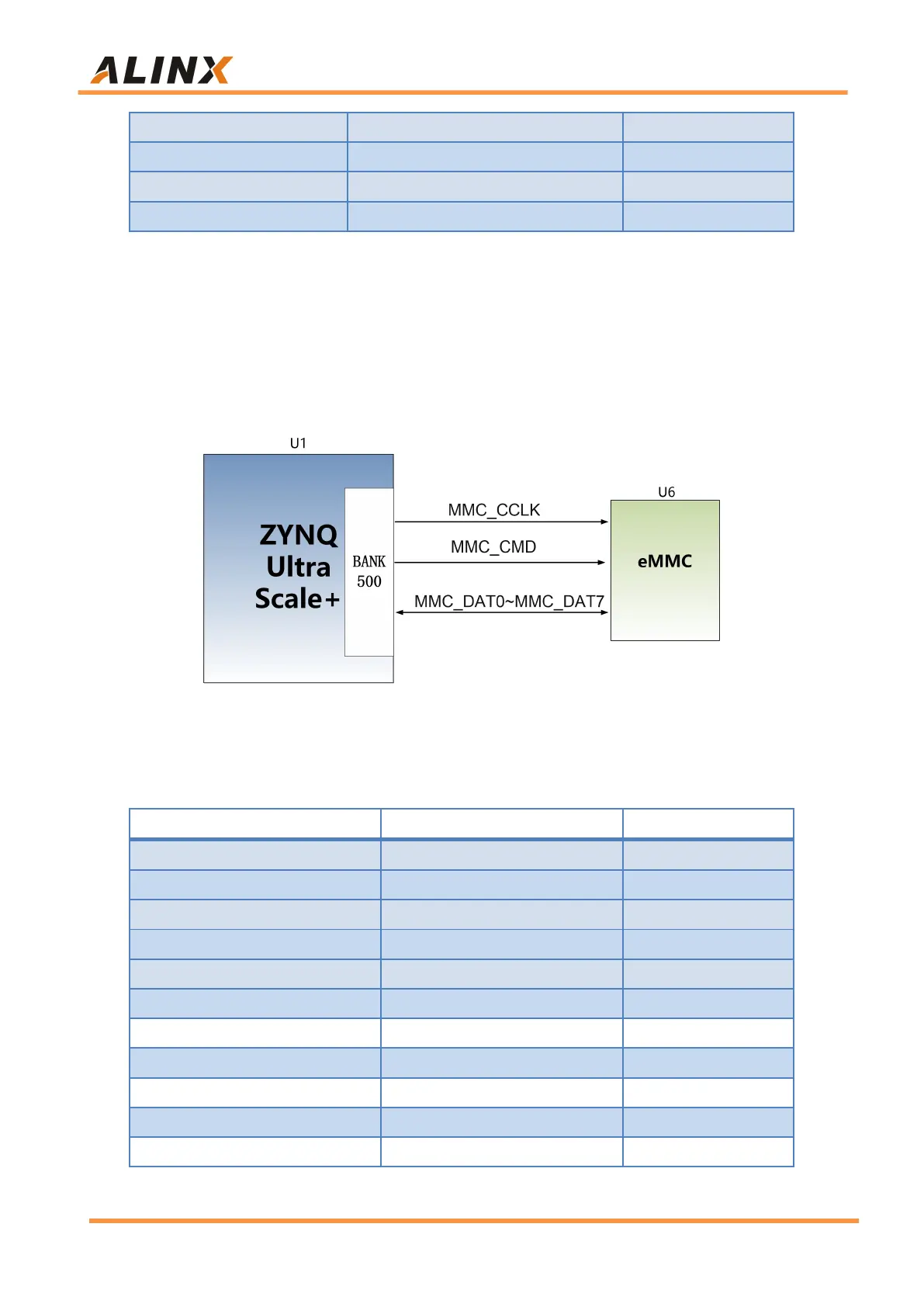
Part 5: eMMC Flash (Only for AXU2CGB)
There is an eMMC FLASH chip with a capacity of 8GB on the AXU2CGB
board. The eMMC FLASH is connected to the GPIO port of the BANK500 of
the PS part of ZYNQ UltraScale+. Figure 5-1 is the eMMC Flash schematic.
Figure 5-1: eMMC Flash Schematic
Configure Chip Pin Assignment:
Signal Name
Pin Name
Pin Number
MMC_DAT0
PS_MIO13_500
AH18
MMC_DAT1
PS_MIO14_500
AG18
MMC_DAT2
PS_MIO15_500
AE18
MMC_DAT3
PS_MIO16_500
AF18
MMC_DAT4
PS_MIO17_500
AC18
MMC_DAT5
PS_MIO18_500
AC19
MMC_DAT6
PS_MIO19_500
AE19
MMC_DAT7
PS_MIO20_500
AD19
MMC_CMD
PS_MIO21_500
AC21
MMC_CCLK
PS_MIO22_500
AB20
MMC_RSTN
PS_MIO23_500
AB18

Related product manuals