ZYNQ Ultrascale + FPGA Board AXU2CGA/B User Manual
Amazon Store: https://www.amazon.com/alinx
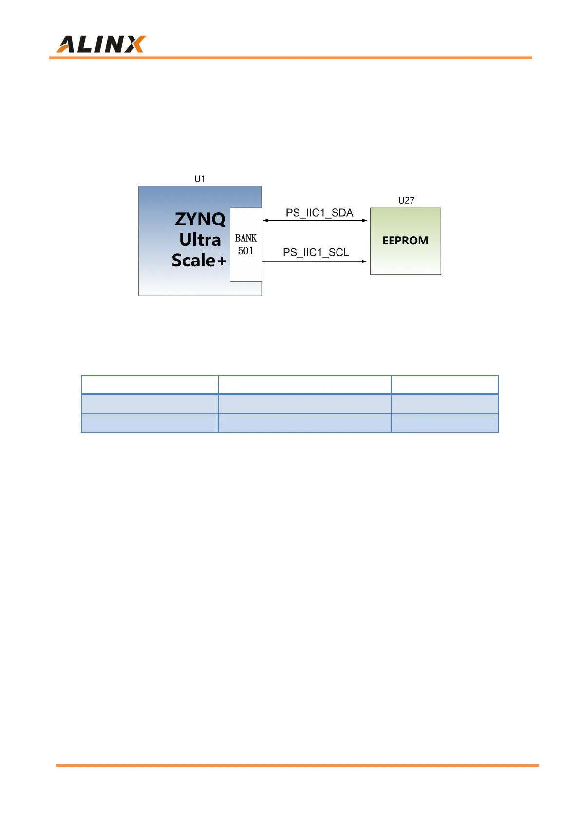
Part 6: EEPROM
The AXU2CGA/B development board has a piece of EEPROM onboard,
the model number is 24LC04. The I2C signal of the EEPROM is connected to
the MIO port of the ZYNQ PS side. Figure 6-1 is EEPROM schematic:
Figure 6-1: EEPROM Schematic
EEPROM Pin Assignment:
Part 7: DP Display Interface
The AXU2CGA/B board has a MINI-type DisplayPort output display
interface, which is used for video image display, and supports up to 4K x
2K@30Fps output. The TX signals of LANE0 and LANE1 of ZU2CG PS MGT
are connected to the DP connector in a differential signal mode. The
DisplayPort auxiliary channel is connected to the MIO pin of the PS. The
schematic diagram of the DP output interface is shown in Figure 7-1: