ZYNQ Ultrascale + FPGA Board AXU2CGA/B User Manual
Amazon Store: https://www.amazon.com/alinx
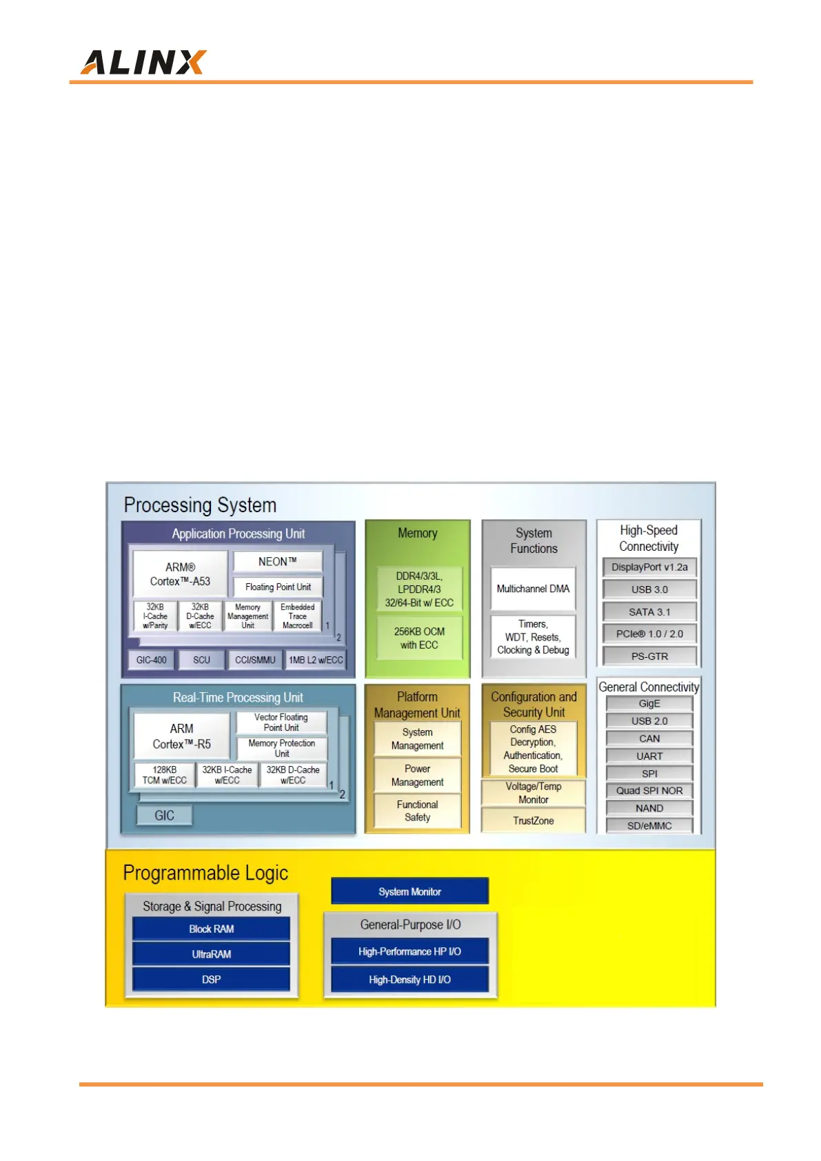
Part 2: ZYNQ Chip
The PS system of the XCZU2CG-1SFVC784E chip integrates two ARM
Cortex™-A53 processors with a speed of up to 1.2Ghz and supports Level 2
Cache; it also contains two Cortex-R5 processors with a speed of up to
500Mhz. The XCZU2CG Chip supports 32-bit or 64-bit DDR4, LPDDR4, DDR3,
DDR3L, LPDDR3 memory chips, with rich high-speed interfaces on the PS
side such as PCIE Gen2, USB3.0, SATA 3.1, DisplayPort; it also supports
USB2.0, Gigabit Ethernet, SD/SDIO, I2C, CAN, UART, GPIO and other
interfaces. The PL end contains a wealth of programmable logic units, DSP and
internal RAM. The overall block diagram of the XCZU2CG chip is shown in the
figure 2-1:
Figure 2-1: Overall Block Diagram of ZU2CG Chip