ZYNQ Ultrascale + FPGA Board AXU2CGA/B User Manual
Amazon Store: https://www.amazon.com/alinx
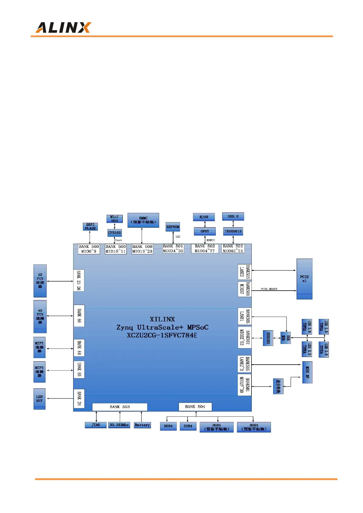
Part 1: AXU2CGA/B Introduction
The AXU2CGA/B Board is characterized by its small size and extensive
peripherals. The main chip is Xilinx's Zynq UltraScale+ MPSoCs CG family chip,
the model is XCZU2CG-1SFVC784E. The PS side of AXU2CGA is mounted
with 2 slices of DDR4 (total 1GB, 32bit) and 1 slice of 256Mb QSPI FLASH.
The PS side of AXU2CGB is equipped with 4 DDR4 (total 2GB, 64bit), one 8GB
eMMC FLASH memory chip and one 256Mb QSPI FLASH.
Peripheral interfaces include 1 MINI DP interface, 4 USB3.0 interfaces, 1
Gigabit Ethernet interface, 1 USB serial port, 1 PCIE interface, 1 TF card
interface, 2 40-pin expansion ports, 2 MIPI Interface, KEYs and LEDs.
The board schematic is as Figure 1-1:
Figure 1-1: Board Schematic