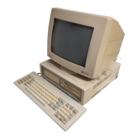
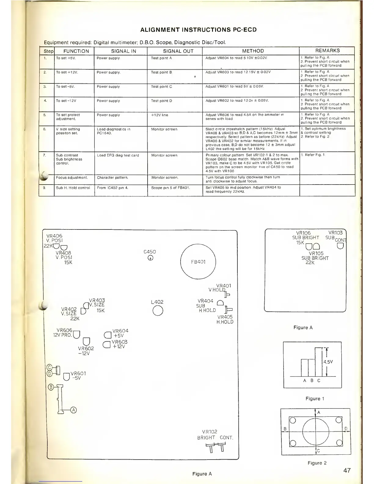
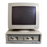
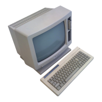
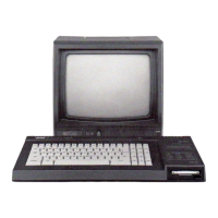
ALIGNMENT INSTRUCTIONS
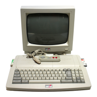
PC-ECD
Equipment required: Digital multimeter; D.B.O. Scope,
Diagnostic Disc/Tool.
Step FUNCTION SIGNAL IN
SIGNAL OUT
METHOD
REMARKS
i.
To set +5V. Power
supply.
Test point
A.
Adjust VR604
to
read 5.10V
±0.02V.
1.
Refer
to
Fig. A.
2.
Prevent short circuit when
pulling the PCB forward.
2 To set +12V.
Power
supply. Test point B.
i
Adjust VR603 to
read
1 2.1
5V ±
0.02V.
1. Refer to
Fig. A,
2.
Prevent short circuit when
pulling the PCB forward.
3.
To
set
-5V.
Power supply. Test point
C.
Adjust VR601 to
read 5V ± 0.05V.
1. Refer to Fig A.
2. Prevent short
circuit when
pulling the PCB forward.
4.
To set -12V. Power supply. Test point
D.
Adjust VR602
to
read 12.0v ±
0.05V.
1. Refer to Fig.
A.
2. Prevent
short circuit when
pulling
the PCB forward.
5.
To
set
protect
adjustment.
Power supply. +
12V
line.
Adjust VR606 to
read 4.5A on the
ammeter in
series with load.
1. Refer
to
Fig.
A.
2.
Prevent short circuit when
pulling the PCB forward.
6.
V. size
setting
possiton
set.
Load diagnostics in
PC1640.
Monitor screen.
Siect circle
Crosshatch pattern (15kHz).
Adjust
VR408 & VR403 so
B,D &
A.C becomes 1 2mm ±
3mm
respectively.
Select pattern
as
before (22kHz).
Adjust
VR406 & VR402
for similar measurements.
If in
previous case, B,D do
not become 1 2 ±
3mm adjust
L402 the
setting will
be
for 1 5kHz.
1. Set
optimum brightness
&
contrast
setting.
2.
Refer
to
Fig. 2.
7.
Sub
contrast
Sub
brightness
control.
Load EFG diag test card. Monitor
screen.
Primary colour pattern. Set VR1
02-1
&
2 to max.
Scope
Q802 base
match. Match A&B wave
forms with
VR1
03,
make C to be
4.5V with VR1
05.
Get
circle
pattern on
the screen monitor +ve
of
C450
to read
4.5V with VR106.
1.
Refer Fig. 1.
^
Focus
adjustment. Character
pattern.
Monitor screen.
Turn focus control
fully clockwise then turn
anti clockwise to
adjust focus.
9.
Sub H.
Hold control. From.lC402 pin 4. Scope
pin
5
of FB401. Set
VR405 to mid
position. Adjust VR404 to
read frequency 22kHz.
VR406
V.
POSI
22K0
VR408
V. POSI
15K
C450
Q
VR402
V.SIZE
22K
VR403
V.SIZE
15K
L402
O
VR401
VHOLtT
VR404
(~^
SUB
"—
J
-
n_
H.HOLD
Jp
VR405
H.HOLD
VR606,
—
.
12V PRO.
\J)
D
1
VR602
-12V
-5V
„VR604
Q
+5V
/—
"
1VR603
LJ +12V
CD-r?
±-®
L5
VR102
BRIGHT CONT.
VR106
VR103
SUB BRIGHT SUB
,5K
DQ
VR105
SUB
BRIGHT
22
K
CONT
O
Figure A
Figure
1
"f
4.5V
I
ABC
A
B
O
/"
"\
°
D
D
V
y
c
c
Figure 2
Figure A
47