AT90S2313
52
Port D
Three I/O memory address locations are allocated for the Port D, one each for the Data Register - PORTD, $12($32), Data
Direction Register - DDRD, $11($31) and the Port D Input Pins - PIND, $10($30). The Port D Input Pins address is read
only, while the Data Register and the Data Direction Register are read/write.
Port D has seven bi-directional I/O pins with internal pull-up resistors, PD6..PD0. The Port D output buffers can sink 20 mA.
As inputs, Port D pins that are externally pulled low will source current if the pull-up resistors are activated.
Some Port D pins have alternate functions as shown in the following Table 19:
When the pins are used for the alternate function the DDRD and PORTD register has to be set according to the alternate
function description.
Port D Data Register - PORTD
Port D Data Direction Register - DDRD
Port D Input Pins Address - PIND
The Port D Input Pins address - PIND - is not a register, and this address enables access to the physical value on each
Port D pin. When reading PORTD, the Port D Data Latch is read, and when reading PIND, the logical values present on the
pins are read.
Table 19. Port D Pins Alternate Functions
Port Pin Alternate Function
PD0 RXD (Receive data input for the UART)
PD1 TXD (Transmit data output for the UART)
PD2 INT0 (External interrupt 0 input)
PD3 INT1 (External interrupt 1 input)
PD4 TO (Timer/Counter0 external input)
PD5 T1 (Timer/Counter1 external input)
PD6 ICP (Timer/Counter1Input Capture pin)
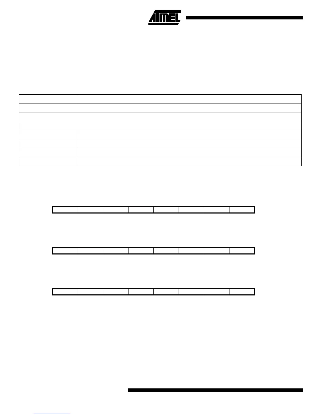
Bit 76543210
$12 ($32) - PORTD6PORTD5PORTD4PORTD3PORTD2PORTD1PORTD0PORTD
Read/Write R R/W R/W R/W R/W R/W R/W R/W
Initial value 0 0 0 0 0 0 0 0
Bit 76543210
$11 ($31) - DDD6 DDD5 DDD4 DDD3 DDD2 DDD1 DDD0 DDRD
Read/Write R R/W R/W R/W R/W R/W R/W R/W
Initial value 0 0 0 0 0 0 0 0
Bit 76543210
$10 ($30) - PIND6 PIND5 PIND4 PIND3 PIND2 PIND1 PIND0 PIND
Read/Write RRRRRRRR
Initial value 0 Hi-Z Hi-Z Hi-Z Hi-Z Hi-Z Hi-Z Hi-Z