AT90S2313
70
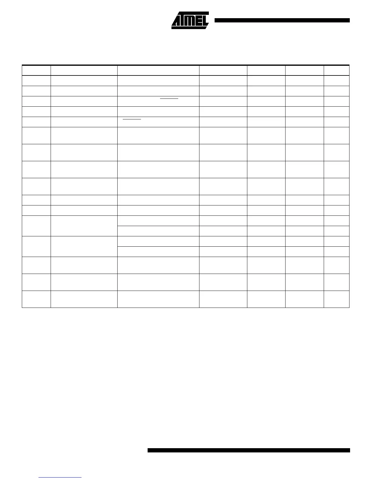
DC Characteristics
Notes: 1. “Max” means the highest value where the pin is guaranteed to be read as low
2. “Min” means the lowest value where the pin is guaranteed to be read as high
3. Although each I/O port can sink more than the test conditions (20mA at Vcc = 5V, 10mA at Vcc = 3V) under steady state
conditions (non-transient), the following must be observed:
1] The sum of all I
OL
, for all ports, should not exceed 200 mA
2] The sum of all II
OL
, for port D0-D5 and XTAL2 should not exceed 100 mA.
3] The sum of all I
OL
, for ports B0-B7 and D6 should not exceed 100 mA.
If I
OL
exceeds the test condition, V
OL
may exceed the related specification. Pins are not guaranteed to sink current greater
than the listed test condition.
4. Although each I/O port can source more than the test conditions (3 mA at Vcc = 5V, 1.5 mA at Vcc = 3V) under steady state
conditions (non-transient), the following must be observed:
1] The sum of all I
OH
, for all ports, should not exceed 200 mA
2] The sum of all I
OH
, for port D0-D5 and XTAL2 should not exceed 100 mA.
3] The sum of all I
OH
, for ports B0-B7 and D6 should not exceed 100 mA.
If I
OH
exceeds the test condition, V
OH
may exceed the related specification. Pins are not guaranteed to source current
greater than the listed test condition.
5. Minimum V
CC
for Power Down is 2V.
T
A
= -40
°
C to 85
°
C, V
CC
= 2.7V to 6.0V (unless otherwise noted)
Symbol Parameter Condition Min Typ Max Units
V
IL
Input Low Voltage (Except XTAL1) -0.5 0.3 V
CC
(1)
V
V
IL1
Input Low Voltage (XTAL1) -0.5 0.1
(1)
V
V
IH
Input High Voltage (Except XTAL1, RESET)0.6 V
CC
(2)
V
CC
+ 0.5 V
V
IH1
Input High Voltage (XTAL1) 0.7 V
CC
(2)
V
CC
+ 0.5 V
V
IH2
Input High Voltage (RESET)0.85 V
CC
(2)
V
CC
+ 0.5 V
V
OL
Output Low Voltage
(3)
(Ports B,D)
I
OL
= 20 mA, V
CC
= 5V
I
OL
= 10 mA, V
CC
= 3V
0.6
0.5
V
V
V
OH
Output High Voltage
(4)
(Ports B,D)
I
OH
= -3 mA, V
CC
= 5V
I
OH
= -1.5 mA, V
CC
= 3V
4.3
2.3
V
V
I
IL
Input Leakage
Current I/O pin
Vcc = 6V, pin low
(absolute value)
1.5 µA
I
IH
Input Leakage
Current I/O pin
Vcc = 6V, pin high
(absolute value)
980 nA
RRST Reset Pull-up Resistor 100 500 kΩ
R
I/O
I/O Pin Pull-Up Resistor 35 120 kΩ
I
CC
Power Supply Current
Active Mode, V
CC
= 3V, 4MHz 3.0 mA
Idle Mode V
CC
= 3V, 4MHz 1.0 mA
I
CC
Power Down Mode
(5)
WDT enabled, V
CC
= 3V 9 15.0 µA
WDT disabled, V
CC
= 3V <1 2.0 µA
V
ACIO
Analog Comparator
Input Offset Voltage
V
CC
= 5V 40 mV
I
ACLK
Analog Comparator
Input Leakage Current
V
CC
= 5V
V
in
= V
CC
/2
-50 50 nA
t
ACPD
Analog Comparator
Propagation Delay
V
CC
= 2.7V
V
CC
= 4.0V
750
500
ns