AT90S4414/8515
42
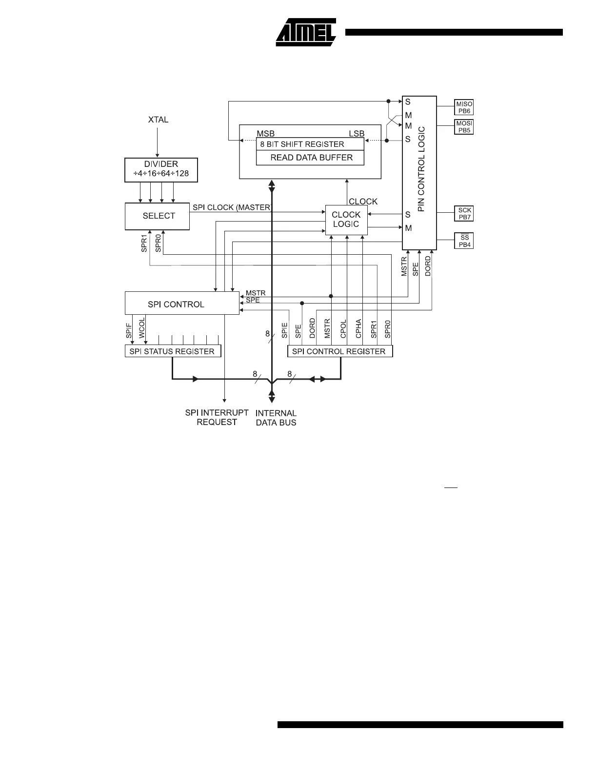
Figure 34. SPI Block Diagram
The interconnection between master and slave CPUs with SPI is shown in Figure 35. The PB7(SCK) pin is the clock output
in the master mode and is the clock input in the slave mode. Writing to the SPI data register of the master CPU starts the
SPI clock generator, and the data written shifts out of the PB5(MOSI) pin and into the PB5(MOSI) pin of the slave CPU.
After shifting one byte, the SPI clock generator stops, setting the end of transmission flag (SPIF). If the SPI interrupt enable
bit (SPIE) in the SPCR register is set, an interrupt is requested. The Slave Select input, PB4(SS
), is set low to select an
individual slave SPI device. The two shift registers in the Master and the Slave can be considered as one distributed 16-bit
circular shift register. This is shown in Figure 35. When data is shifted from the master to the slave, data is also shifted in
the opposite direction, simultaneously. This means that during one shift cycle, data in the master and the slave are
interchanged.

 Loading...


