Physical Interface AW00123401000
38 Basler ace USB 3.0
For more information about GPIO pin assignments and pin numbering, see Section 5.2.1 on
page 28.
For more information about setting the GPIO line operation, see a following version of the manual.
1
6
3
4
2
5
FPGA Input
+3.3 VDC
(Typical)
Input Buffer
Camera
Your
Gnd
6-pin
Receptacle
Logic Gate
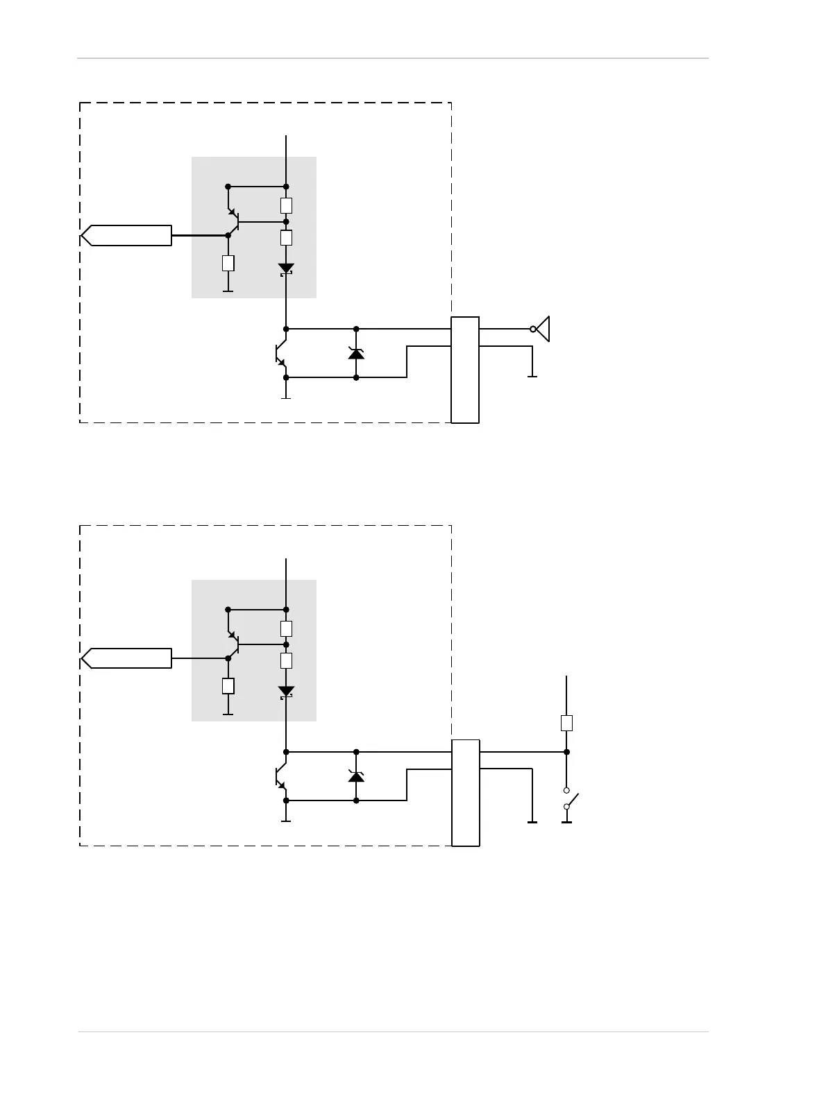
Fig. 20: Direct-coupled GPIO Line Schematic with the GPIO Line Set as an Input and with a Typical External Circuit
Using a Logic Gate (Illustration for Pin 1 as an Example; Simplified)
1
6
3
4
2
5
FPGA Input
+3.3 VDC
(Typical)
Input Buffer
Camera
Your
Gnd
6-pin
Receptacle
+3.3 V ... +5.0 V
Fig. 21: Direct-coupled GPIO Line Schematic with the GPIO Line Set as an Input and with a Typical External Circuit
(Illustration for Pin 1 as an Example; Simplified)