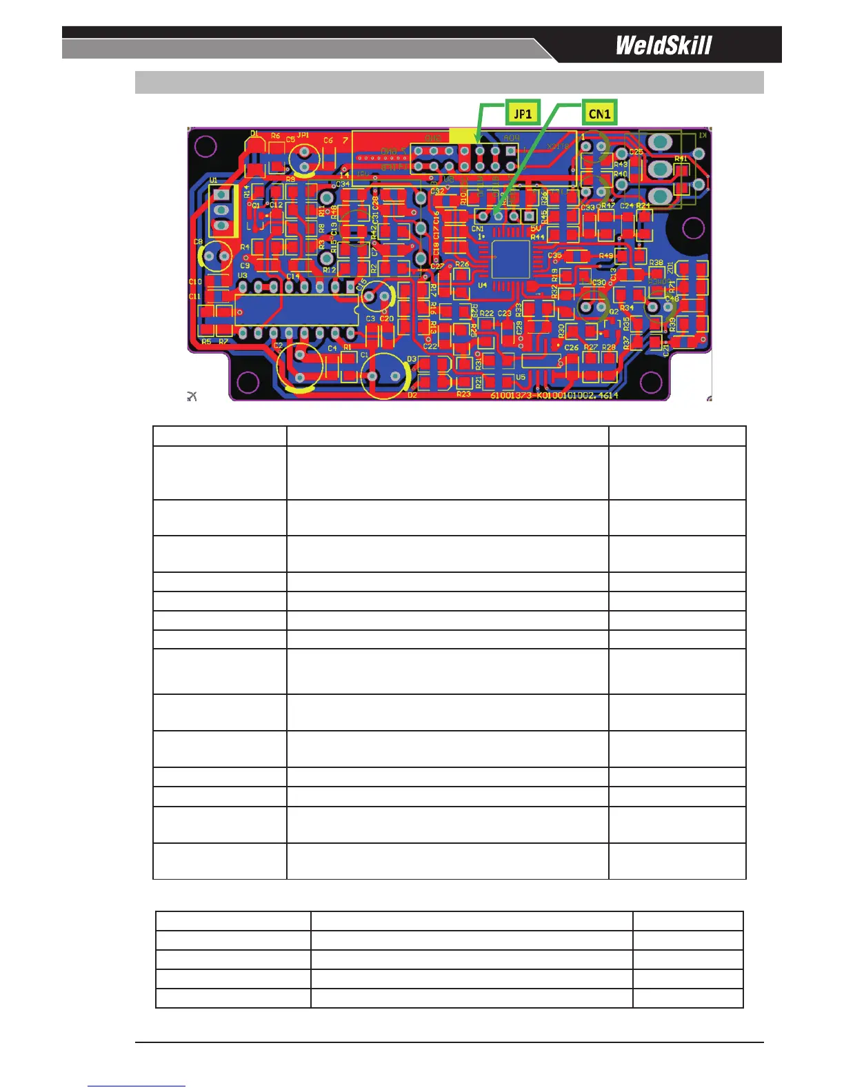
JP1 Header Pin Pin function Signal
1
PDA-SHORT signal which is used to detect a short cir-
cuit at the welding terminals 5V = No short at welding
terminals; 0.2V = Short at welding terminals
5 VDC
2
OUTA IGBT 1/2/3/4 PWM drive signal, 15V p-p square
wave signal
15 VDC pk
3
OUTB IGBT 1/2/3/4 PWM drive signal, 15V p-p square
wave signal
15 VDC pk
4
Vcc-A = +15V supply +15 VDC
5
0V 0 VDC
6
0V 0 VDC
7
0V 0 VDC
8
Thermostat signal from Inverter PCB
2.5 VDC (Tr.1 closed)
5 VDC (Tr.1 open)
9
OUTA IGBT 1/2/3/4 PWM drive signal, 15V p-p square
wave signal
15 VDC pk
10
OUTB IGBT 1/2/3/4 PWM drive signal, 15V p-p square
wave signal
15 VDC pk
11
Vcc-A = +15V supply 15 VDC
12
+5V supply to Inverter PCB +5 VDC
13
PEAK-IFB Primary current feedback signal from
Inverter PCB
14
PEAK-IFB Primary current feedback signal from
Inverter PCB
Table 12-6 JP1 Header pin function (connects to JP1 header on Inverter PCB)
CN1 Header Pin Pin function Signal
1 +5V supply +5 VDC
2
Programming pin
Digital Signal
3
0V 0 VDC
4
Reset pin Digital Signal
Table 12-7 CN1 Header pin function (used for uploading program to Control PCB)