Schematic Diagrams
B - 1
B.Schematic Diagrams
Appendix B: Schematic Diagrams
Table B - 1
SCHEMATIC
DIAGRAMS
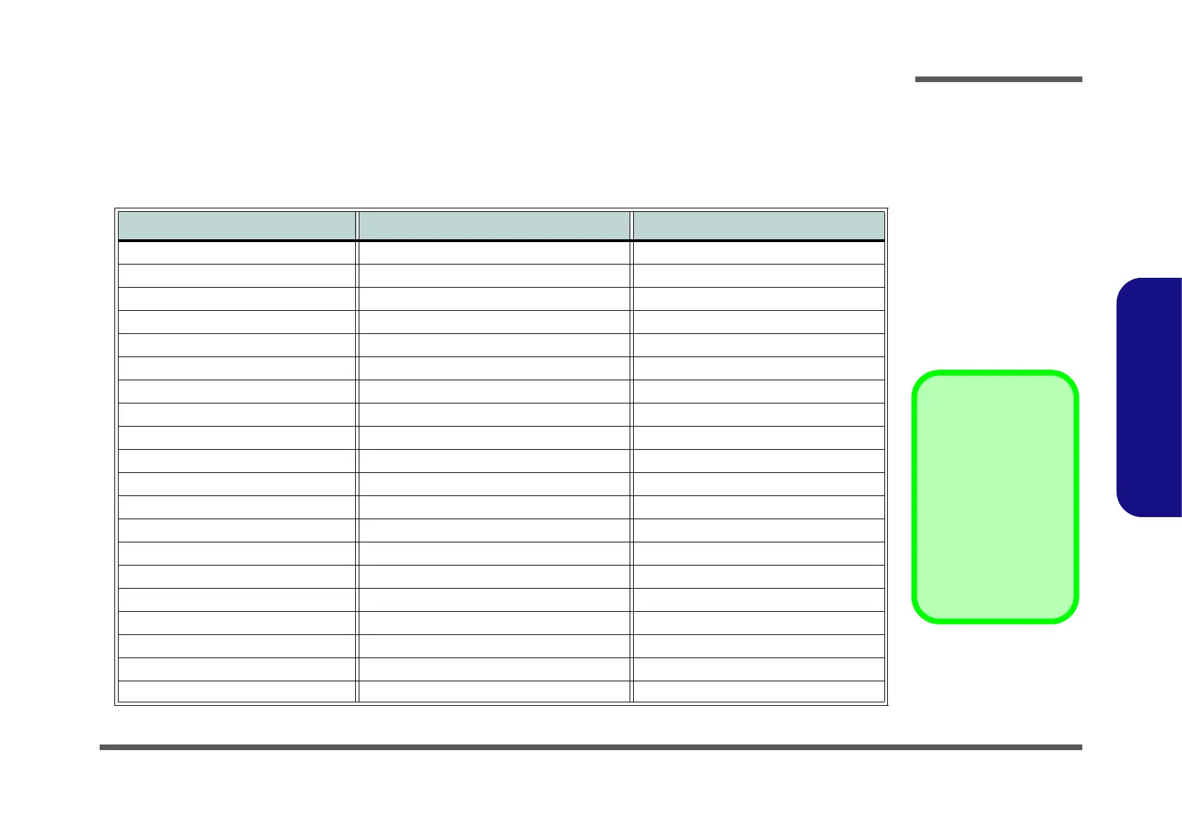
This appendix has circuit diagrams of the NV40MZ / NV41MZ notebook’s PCB’s. The following table indicates where
to find the appropriate schematic diagram.
Diagram - Page Diagram - Page Diagram - Page
System Block Diagram - Page B - 2 NVIDIA Power Sequence - Page B - 22 Conn Fan, CCD, TP, LED KB - Page B - 42
Processor 1/12 - Page B - 3 NVIDA GPIO Level Shift - Page B - 23 AC-In - Page B - 43
Processor 2/12 - Page B - 4 VGA PWR, GND, NC - Page B - 24 LED, LID SW - Page B - 44
Processor 3/12 - Page B - 5 VGA NVVDD Coupling - Page B - 25 VCCIN - Page B - 45
Processor 4/12 - Page B - 6 DDR4 SO-DIMM A - Page B - 26 VCCIN Aux - Page B - 46
Processor 5/12 - Page B - 7 DDR4 SO-DIMM B - Page B - 27 1.8VA, 1.5VS - Page B - 47
Processor 6/12 - Page B - 8 Panel - Page B - 28 3.3V, 5V, 3VS, 5VS, CTL - Page B - 48
Processor 7/12 - Page B - 9 HDMI - Page B - 29 V1.05A / VNN - Page B - 49
Processor 8/12 - Page B - 10 Audio Codec - Page B - 30 VDD3, VDD5 - Page B - 50
Processor 9/12 - Page B - 11 M Key PCIE SSD - Page B - 31 VDDQ, VDDQ_VTT, 1.8VA - Page B - 51
Processor 10/12 - Page B - 12 USB Charger, TPM - Page B - 32 2.5V, VCCST, VCCSTG - Page B - 52
Processor 11/12 - Page B - 13 USB, LED - Page B - 33 Charger, AC-In - Page B - 53
Processor 12/12 - Page B - 14 IT5570 - Page B - 34 3.3VA, NV3V3 - Page B - 54
VGA PCI-E, Straps, XTAL - Page B - 15 RTL8111G - Page B - 35 NVVDD1 - Page B - 55
VGA Frame Buffer Interface - Page B - 16 WLAN/BT - Page B - 36 NVVDD2 - Page B - 56
VGA Frame Buffer A - Page B - 17 RTS5227S - Page B - 37 PEX_VDD - Page B - 57
VGA Frame Buffer A - Page B - 18 Type-C USB3.0 - Page B - 38 FBVDDQ - Page B - 58
VGA Frame Buffer B - Page B - 19 Type-C, Retimer 1/2 - Page B - 39 DGPU Power Measurement - Page B - 59
VGA Frame Buffer B - Page B - 20 Type-C, Retimer 2/2 - Page B - 40 1V8_AON/RUN, NV3V3 - Page B - 60
VGA I/O - Page B - 21 Type-C Con - Page B - 41 Power Sequence - Page B - 61
Version Note
The schematic dia-
grams in this chapter
are based upon version
6-71-NV400-D02A. If
your mainboard (or oth-
er boards) are a later
version, please check
with the Service Center
for updated diagrams
(if required).