Chapter 7 Selection guide of inverter Accessory VFD500 high performance vector control frequency inverter user
manual
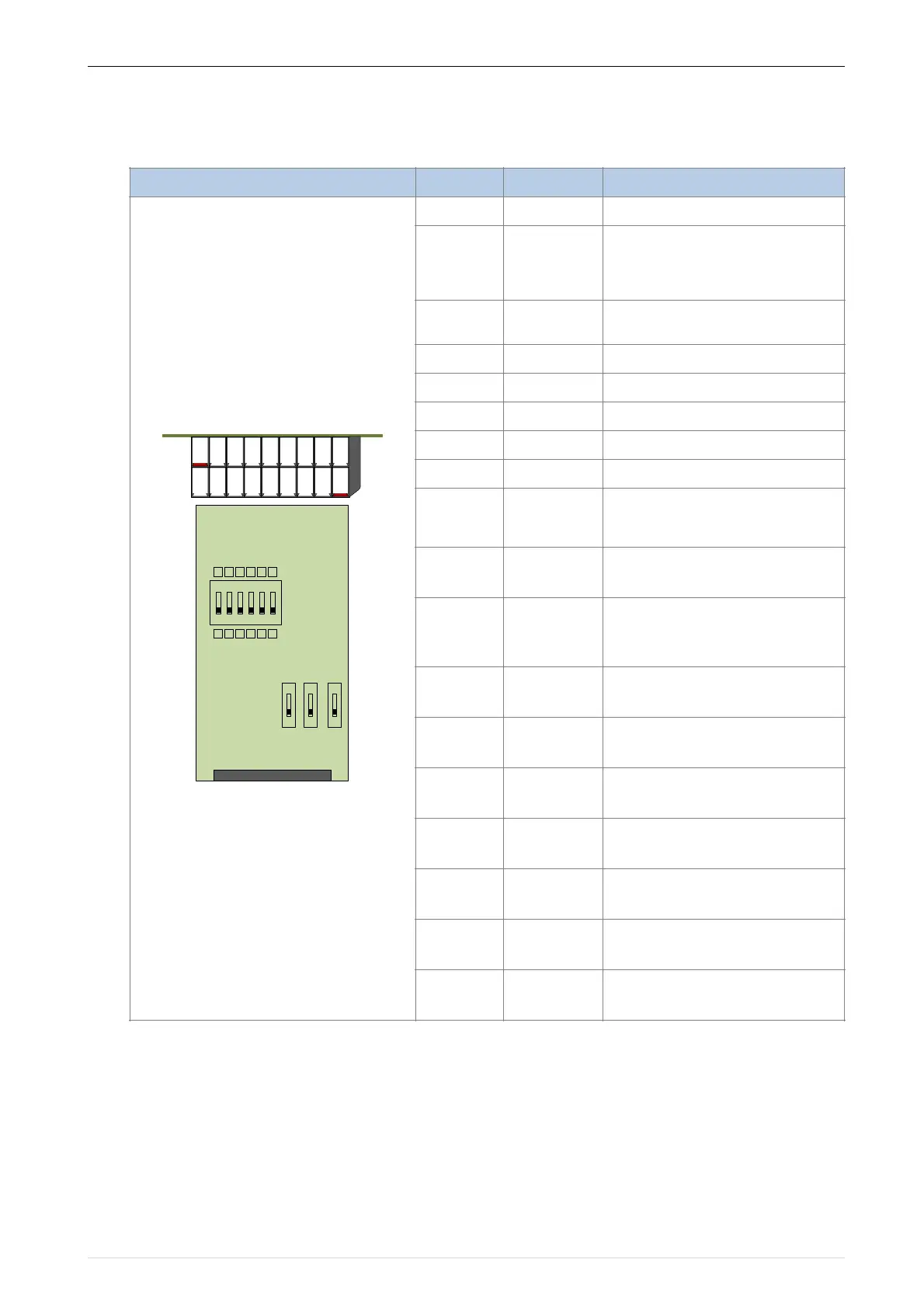
The input signal of the VFD500-PG-INC2 crossover PG card can be differential or open collector
type, selected by the DIP switch; there are two sets of output signals, open collector type and
differential output type; The card's port definition is shown in the table below.
Chart 7-8 Incremental encoder PG card with frequency division (VFD500-PG-INC2) port definition
In the schematic diagram of the crossover card in Table 7-5, the dial switch indicates bit 0~bit5 of
the frequency division number from right to left, the frequency division range is 0~63, and the
frequency division number is set to 0 and 1 when there is no frequency division.
(3)Resolver PG card
Chart 7-9 Resolver PG Card (VFD500-PG-RT1) Interface Definition
Power output for powering the
encoder
5V ± 2%, maximum 200mA
12V±5%, maximum 200mA
Power supply common terminal and
signal
Z signal crossover output (NPN
open collector type)
B-phase pulse frequency
dividing output (NPN open
collector type)
Phase A pulse divider output
(NPN open collector type)
Z signal crossover output Z-
(differential output type)
Z signal crossover output Z+
(differential output type)
B-phase pulse divider output
B- (differential output type)
B-phase pulse divider output
B+ (differential output type)
Phase A pulse divider output A-
(differential output type)
Phase A pulse divider output A+
(differential output type)
 Loading...