DESIGNER’S HANDBOOK 4189350049C EN Page 120 of 206
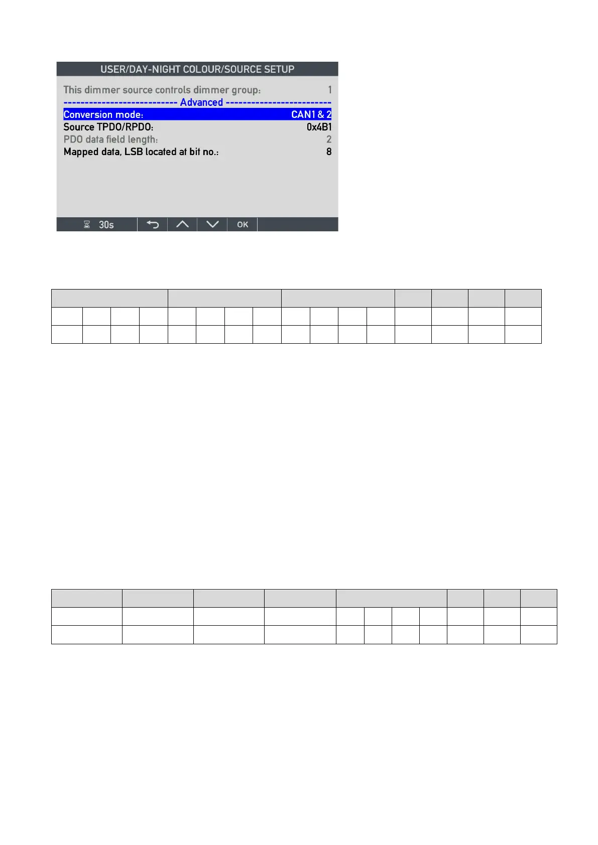
The following menu is available:
The PDO may be received via CAN1, CAN2 or
both
The COB-ID of the PDO used for data transfer
may be changed.
Also, the mapping of the 2 input bits in the 64 bit
data frame of the TPDO may be changed via
menu.
Example 1:
TPDO containing all 9 colour shift parameter set in the 3 first bytes
Byte 0: Gr. 1 with LSB located at bit 0, Data in bit 0 1
Gr. 2 with LSB located at bit 2, Data in bit 2 3
Gr. 3 with LSB located at bit 4, Data in bit 4 5
Gr. 4 with LSB located at bit 6, Data in bit 6 7
Byte 1: Gr. 5 with LSB located at bit 8, Data in bit 8 9
Gr. 6 with LSB located at bit 10, Data in bit 10 11
Gr. 7 with LSB located at bit 12, Data in bit 12 13
Gr. 8 with LSB located at bit 14, Data in bit 14 15
Byte 2: Gr. 9 with LSB located at bit 16, Data in bit 16 17
Example 2:
It is also possible to combine dimmer level and colour shift data in the same TPDO. In this example, data for
dimmer group 1 to 4 is located in byte 0 to 4:
Byte 0: Dimmer Gr. 1 with LSB located at bit 0, Data in bit 0 to 7
Byte 1: Dimmer Gr. 2 with LSB located at bit 8, Data in bit 8 to 15
Byte 2: Dimmer Gr. 3 with LSB located at bit 16, Data in bit 16 to 23
Byte 3: Dimmer Gr. 4 with LSB located at bit 24, Data in bit 24 to 31
Byte 4: Colour sh. Gr. 1 with LSB located at bit 32, Data at bit 32, 33
Colour sh. Gr. 2 with LSB located at bit 34, Data at bit 34, 35
Colour sh. Gr. 3 with LSB located at bit 36, Data at bit 36, 37
Colour sh. Gr. 4 with LSB located at bit 38, Data at bit 38, 39
 Loading...