below:
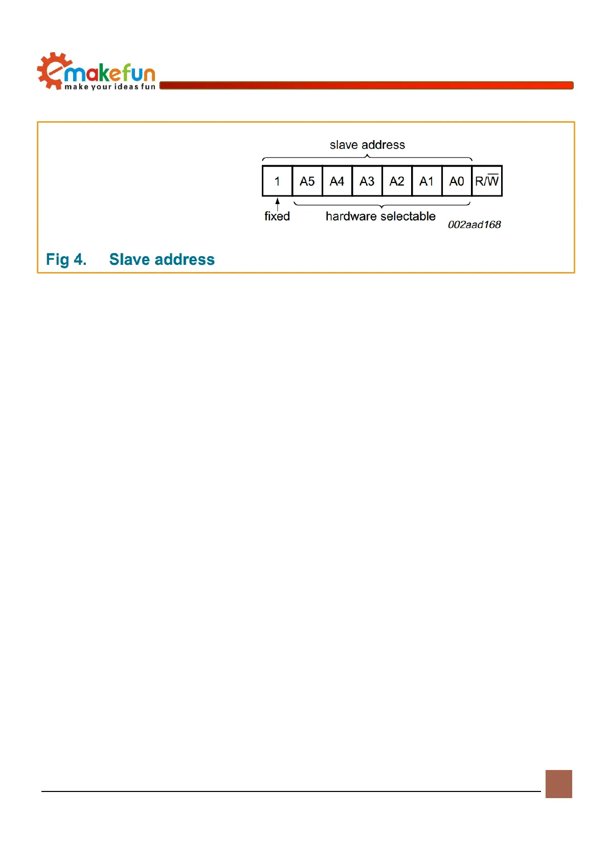
Figure 6-1 Device address schematic
For detailed use of the chip, please refer to《MotorDriverBoard\Datasheet\PCA9685.pdf》
TB6612FNG Introduction
The PS2X&Motor Driver Board uses TB6612FNG to drive the motor. The TB6612FNG has a high-current
MOSFET-H bridge structure, dual-channel circuit output, and a continuous drive current of up to 1.2 A per
channel. The peak current is 2A/3.2 A (continuous pulse/single pulse). 4 kinds of motor control modes:
forward/reverse/brake/stop; standby state; PWM supports frequency up to 100 kHz; on-chip low-voltage
detection circuit and thermal shutdown protection circuit, main pin function of TB6612FNG: AINl/AIN2
BIN1/BIN2, PWMA/PWMB are control signal input terminals; AO1/A02, B01/B02 are 2 motor control
output terminals; STBY is normal working/standby state control pin; VM (4.5~15 V) and VCC ( 2.7 to 5.5
V) are the motor drive voltage input and the logic level input, respectively.
In the Arduino, the analog voltage cannot be output, and only the digital voltage value of 0 or 5V can be
output. We use the high-resolution counter to modulate the square wave's duty cycle to the level of a specific
analog signal to encode. The PWM signal is still digital because at any given time, the full-scale DC supply
is either 5V (ON) or 0V (OFF). The voltage or current source is applied to the analog load in a repeating
pulse sequence of ON or OFF. When the DC power is applied to the load, the power is disconnected when
the power is turned off. Any analog value can be encoded using PWM as long as the bandwidth is sufficient.
The output voltage value is calculated by the on and off times. Output voltage = (on time / pulse time) *
maximum voltage value, Figure 6-2 is the voltage corresponding to the pulse change.