3 Application Interface
Copyright © Fibocom Wireless Inc. 33
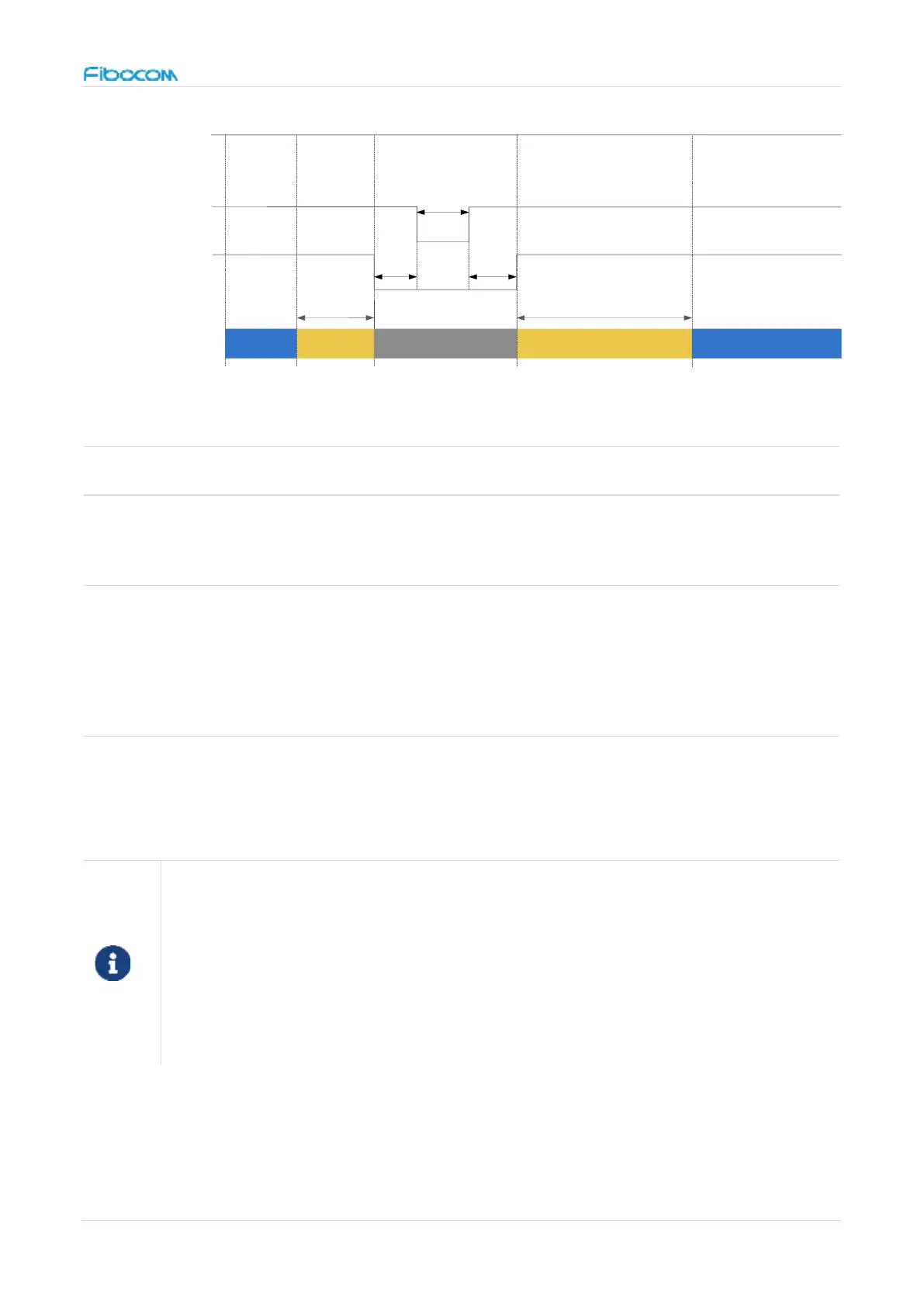
+3.3V
RESET#
Module State
InitializationActivation
FCPO#
typical TBD
Activation
toff
Finalization OFF
AT+CPWROFF
toff1 ton1
tsd
Figure 11. Reset timing 2
nd
FCPO# should be asserted after RESET#,
refer section 3.3.2
Time to allow the WWAN module to fully
discharge any residual voltages before the pin
could be de-asserted again. This is required for
both Pre-OS as well as Runtime flow
RESET# should be de-asserted after FCPO# assert
to high,
refer section 3.3.1.2
RESET# is a sensitive signal, it’s recommended to add a filter capacitor close
to the module. In case of PCB layout, the RESET# signal lines should keep
away from the RF interference and protected by GND. Also, the RESET# signal
lines shall neither near the PCB edge nor route on the surface planes to avoid
module from reset caused by ESD problems.
 Loading...