Do you have a question about the Fibocom L610 Series and is the answer not in the manual?
Describes electrical characteristics, RF performance, dimensions, and application environment of L610 modules.
Provides safety guidelines for personal safety and product protection, including driving, flight, and medical facility precautions.
Introduces L610 modules as wideband wireless terminal products for various network formats and multi-bands.
Details operating bands, data transmission rates, power supply, temperature, power consumption, physical characteristics, and interface.
Shows the main hardware features of L610 module, including baseband and RF features.
Describes the different operating modes of the module: Idle, Talk/Data, and Airplane.
Describes the LCC 80PIN+LGA 64PIN packaging and its pin distribution.
Defines the function, I/O, level, reset value, and description for each pin.
Details the power interfaces of L610 modules, including VBAT_RF, VBAT_BB, VDD_EXT, and GND.
Explains that L610 modules need to be powered by the VBAT pin and provides recommended power design.
Explains the 1.8V output through VDD_EXT for digital circuits and its logic level definition.
Details the power consumption of L610 module in different modes like Ioff, Isleep, and Igsm-rms.
Provides two control signals for power on/off and reset operations.
Defines the RESET_N pin for hardware reset, requiring a pull-down for 100ms.
Defines the PWRKEY pin for power on/off, requiring a minimum low level duration of 2s for power on.
Explains how to power on the module using the PWRKEY pin with reference circuits.
Provides reference circuits for controlling the PWRKEY pin using OC/OD drive or a button.
Illustrates the timing control diagram for powering on the module.
Describes how to enable automatic power-on by connecting PWRKEY to ground.
Details three shutdown modes: Low voltage, Hardware, and AT shutdown.
Shows the timing control diagram for shutting down the module.
Explains how to reset the module using hardware or AT commands.
Illustrates the timing control for the RESET_N signal.
Details the USB interface capabilities and specifications.
Defines the USB_DM, USB_DP, and USB_VBUS pins and their functions.
Provides information on the USIM interface and its support for different SIM types.
Lists the USIM pins and their corresponding functions: DATA, CLK, RESET, VDD, and PRESENCE.
Shows reference designs for SIM card slots with and without detection signals.
Details the design requirements for a SIM card slot with detection functionality.
Describes the configuration for a SIM card slot without detection.
Explains the SIM hot plug function and its configuration via AT commands.
Outlines design rules for SIM circuit to meet EMC, ESD, and anti-interference standards.
Details the UART interface, including definition and application.
Defines the main serial port, UART3, and debug serial ports and their baud rates.
Illustrates reference circuits for serial port level translation between module and host.
Describes the status indicator signals, focusing on NET_MODE.
Describes the NET_MODE signal as a network status indicator with different flash patterns.
Explains how to manage low power consumption modes.
Explains how to enter flight mode using hardware or AT command control.
Refers to another document for details on sleep mode.
Details the ADC interfaces and their specifications.
Details the three ADC interfaces (ADCO, ADC1, ADC2) and their voltage ranges and accuracy.
Provides information on the analog audio interface.
Lists supported models for analog audio interface.
Defines the pin assignments for MIC, SPK, and headphone outputs.
Provides recommendations for filtering noise in TDD operations.
Shows the reference circuit for the differential microphone input.
Displays reference circuits for speaker output.
Explains how to enter download mode for module upgrades via USB.
Explains how to enter download mode for module upgrades via USB.
Lists the operating bands for L610 modules, including Tx and Rx frequencies.
Details the RF output power for L610 modules across different bands and modes.
Details the RF receiving sensitivity for GSM and LTE bands.
Provides guidelines for RF PCB layout and design.
Recommends U.FL-R-SMT-1 connector and RF adapter cable for antenna connection.
Covers WIFI and Bluetooth functionalities, including sensitivity and output power.
Shows WIFI/BT receiving sensitivity for different modes and their performance metrics.
Details GNSS functionality, including power consumption and test results.
Details GNSS power consumption and test results for fixing and tracking.
Provides guidelines for antenna design and performance.
Defines antenna efficiency and recommends a minimum of 40% (-4dB).
Explains S11/VSWR as a measure of antenna matching, recommending S11 < -10dB.
Defines polarization and recommends linear polarization.
Describes radiation pattern and recommends PIFA or IFA antennas.
Explains gain and directivity, recommending a gain ",5 2.5dBi.
Provides suggestions for controlling interference from PCB components and layout.
Lists requirements for the L610 Module Main Antenna.
Specifies the voltage ranges for power supply and digital/analog I/O interfaces.
Recommends operating temperature range (-30 to +75°C) and storage conditions.
Details electrical characteristics of interfaces in operating status.
Details tests for low/high temperature storage, shock, humidity, and vibration.
Covers ESD protection considerations and allowable discharge ranges for different parts.
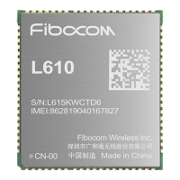
Shows the physical appearance of the L610 module, top and bottom views.
Provides detailed structural dimensions of the L610 module in millimeters.
Refers to another guide for module stencil design, solder paste, and furnace temperature control.
| Brand | Fibocom |
|---|---|
| Model | L610 Series |
| Category | Control Unit |
| Language | English |