Do you have a question about the Fibocom L850-GL and is the answer not in the manual?
Describes electrical characteristics, RF performance, dimensions, and application environment of L850.
Lists the standards the product design complies with.
Lists related documents for further reference.
Introduces L850 as an integrated 4G WWAN module with M.2 form factor.
Details technical specifications including operating band, data transmission, power, temperature, and interfaces.
Provides warnings related to module operation and performance.
Federal Communication Commission Interference Statement.
Industry Canada statement regarding interference and compliance.
EU Regulatory Conformance and Declaration of Conformity.
Describes the standard M.2 Key-B interface of the L850 module.
Provides a detailed pin map for the M.2 interface.
Defines the function and type of each pin in the M.2 interface.
Explains the power supply design and connection for the module.
Defines the 1.8V and 3.3V logic level definitions for the module.
Explains the module start-up process and circuit.
Details the circuit design for module start-up controlled by AP.
Illustrates the timing sequence for module start-up.
Details the PCIe 1.0 interface and data transmission channel.
Defines pins related to the PCIe interface.
Shows reference circuit and PCB layout rules for PCIe interface.
Defines pins related to USB 2.0 and USB 3.0 interfaces.
Shows the reference circuit for USB 2.0 interface.
Shows the reference circuit for USB 3.0 interface.
Defines the pins related to the USIM interface.
Shows reference circuit designs for N.C. and N.O. SIM card slots.
Details the function of the LED#1 signal for status indication.
Explains the W_DISABLE1# pin for RF network enable/disable.
Describes the Body SAR function using the DPR pin.
Details RF interface functionality and connectors.
Describes the function of Main and Diversity antenna connectors.
Lists frequency range and characteristic impedance of RF connectors.
Shows the dimensions of the M.2 module RF connectors.
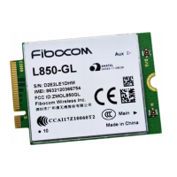
Shows the appearance of the L850 module.
Details the structural dimensions of the L850 module.
Specifies the recommended storage life of the module.
Details the tray packaging process for the module.
Provides the dimensions of the pallet for tray packaging.
| Chipset | Intel XMM 7360 |
|---|---|
| Form Factor | M.2 |
| LTE Category | Cat 9 |
| LTE Download Speed | 450 Mbps |
| LTE Upload Speed | 50 Mbps |
| 3G Bands | B1/B2/B4/B5/B8 |
| Operating Temperature | -10°C to +55°C |
| GNSS | GPS, GLONASS, BeiDou, Galileo |
| Storage Temperature | -40°C to +85°C |
| SIM Interface | 1.8V/3.0V |
| LTE Bands | B1/B2/B3/B4/B5/B7/B8/B12/B13/B17/B18/B19/B20/B26/B28/B29/B30/B66 |
| Operating Voltage | 3.135V to 4.4V |
| Dimensions | 30.0mm x 42.0mm x 2.3 mm |
| Interfaces | USB 2.0 |
| Power Supply Voltage | 3.135V to 4.4V |
| Operating Systems Support | Linux, Android, Windows |
| Certifications | FCC, IC, PTCRB, GCF, CE, RCM |