Do you have a question about the Fibocom L850-GL Series and is the answer not in the manual?
Introduces the hardware functions of L850 modules and assists developers.
Lists the standards the product design complies with for conformance.
Lists additional documents for further technical information and guidance.
Details operating bands, GNSS, LTE, UMTS, data transmission, and physical characteristics of the module.
Lists Carrier Aggregation (CA) combinations supported by different L850 product models.
Illustrates the peripheral applications for the L850 module through a block diagram.
Shows the main hardware functions of the L850 module, covering baseband and RF.
Describes the standard M.2 Key-B interface used by the L850 module, detailing its 75 pins.
Provides a detailed pin map for the M.2 interface, listing pin numbers and their functions.
Details the function, I/O, reset value, and type for each pin of the M.2 interface.
Explains the power interface, input voltage requirements, and power supply design considerations.
Details the power supply design and recommended filter capacitor configurations for stable operation.
Defines the 1.8V and 3.3V logic level parameters for signal integrity.
Presents the power consumption figures for various operating modes and bands.
Describes the control signals for module power on/off and reset operations.
Details the module start-up process, including circuit design and timing.
Shows the recommended circuit for module start-up controlled by the Application Processor.
Illustrates the timing sequence required for a successful module start-up.
Explains the module shutdown procedures, control signals, and timing.
Describes the module reset functionality, recommended circuit designs, and timing.
Discusses PCIe link states (D0 L1.2, D3cold L2) and their impact on power consumption.
Details the D0 L1.2 PCIe link state, including its timing and power implications.
Explains the D3cold L2 PCIe link state and wake-up mechanisms from host or modem.
Provides recommended timing applications for different system states in Win10 and other OS.
Covers the Inter-Process Communication (IPC) interfaces, specifically PCIe and USB for data.
Describes the PCIe Gen1 interface, its initialization, and port mapping for data and GNSS.
Defines the specific pins related to the PCIe interface and their functions.
Shows the reference circuit for the PCIe interface and outlines PCB layout rules.
Details the USB2.0 and USB3.1 Gen1 interface capabilities and applications.
Defines the pins associated with the USB interfaces (USB 2.0 and USB 3.0).
Shows the reference circuit for the USB 2.0 interface.
Shows the reference circuit for the USB 3.0 interface.
Describes the built-in USIM card interface, supporting 1.8V and 3V SIM cards.
Lists the pins dedicated to the USIM card interface and their functions.
Illustrates the circuit designs for both N.C. (Normally Closed) and N.O. (Normally Open) SIM card slots.
Explains the SIM card hot-plug functionality and its configuration via AT commands.
Provides design guidelines for the USIM circuit to ensure stable operation and meet EMC/ESD standards.
Describes the module's status indicator signals like LED, WOWWAN#, and TX_BLANKING.
Details the LED#1 signal's behavior for indicating RF function status (On/Off).
Explains interrupt signals for controlling RF network and GNSS functions.
Describes the W_DISABLE1# pin for enabling/disabling the WWAN RF function and entering flight mode.
Explains the BodySAR function that lowers emission power based on proximity detection.
Details the clock interface, specifically its 26MHz clock output capability.
Covers ANT Tunable interfaces (MIPI, GPO) for flexible LTE antenna configuration.
Details pins used for M.2 module configuration, defining WWAN-PCIe and USB3.1 interface types.
Describes the RF connectors for external antenna connection and their functionality.
Explains the function of the Main (M) and Diversity/GNSS (D/G) RF connectors.
Lists the rated frequency range and characteristic impedance of the RF connectors.
Provides the part number and physical dimensions of the M.2 RF connectors.
Details the correct procedure for mating and unmating RF connectors using a pulling jig.
Lists all supported operating bands for the L850 module, including Tx/Rx frequencies.
Shows the transmitting power output for each supported band across WCDMA, LTE FDD, and LTE TDD modes.
Details the receiver sensitivity performance for each band, crucial for signal reception.
Describes the GNSS feature, including support for GPS, GLONONASS, BDS, and their performance metrics.
Provides antenna design requirements, including bandwidth considerations for various frequency bands.
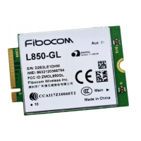
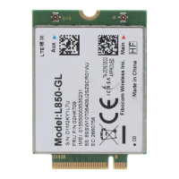
Shows the visual appearance of the L850 module from top and bottom views.
Details the structural dimensions of the L850 module in millimeters, shown in Top, Side, and Bottom views.
Describes the L850 M.2 module's interface model type, including dimensions and keying.
Specifies the recommended M.2 connector part number and dimensions for host connection.
Covers recommended storage conditions and the module's storage life.
Specifies the recommended storage conditions and the resulting storage life of 12 months.
Details the tray sealed packing method combined with outer packaging for module protection.
Explains the tray packaging process, including quantities and arrangement for modules.
Provides the pallet size dimensions for the L850 module packaging.
| Category | GSM/GPRS Modules |
|---|---|
| Model | L850-GL |
| Form Factor | M.2 |
| Operating Temperature | -10°C to +55°C |
| Storage Temperature | -40°C to +85°C |
| GSM Bands | 850/900/1800/1900MHz |
| GNSS | GPS, GLONASS, BeiDou, Galileo |
| Interface | USB 2.0, UART, PCM, I2C, GPIO |
| Operating Voltage | 3.135V to 4.4V |
| LTE FDD | B1, B2, B3, B4, B5, B7, B8, B12, B13, B17, B18, B19, B20, B25, B26, B28, B29, B30, B66 |
| LTE TDD | B38/B39/B40/B41 |
| WCDMA | B1, B2, B4, B5, B8 |
| AT Command Set | 3GPP TS 27.007 |
| Certifications | CE, FCC, GCF, PTCRB |