Reproduction forbidden without Fibocom Wireless Inc. written authorization - All Rights Reserved.
L850-GL Hardware User Manual Page 23 of 54
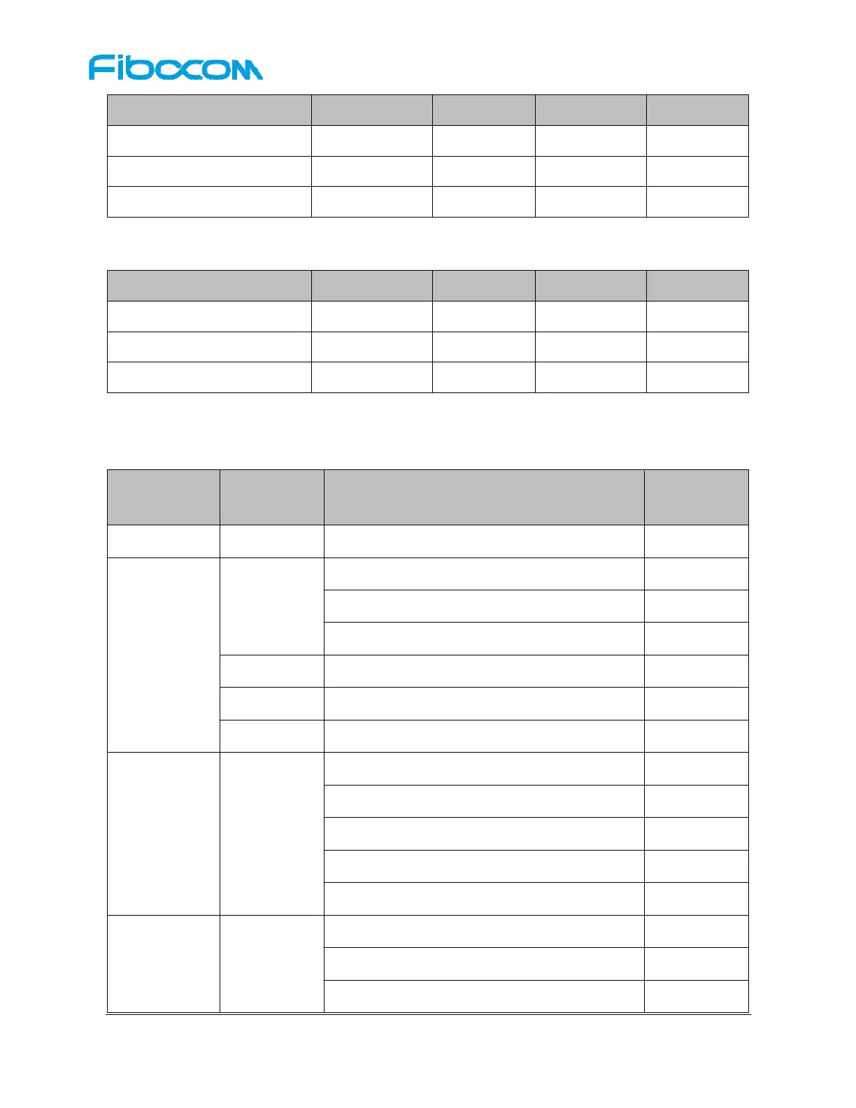
Parameters Minimum Typical Maximum Unit
1.8V logic level 1.71 1.8 1.89 V
V
IH
1.3 1.8 1.89 V
V
IL
-0.3 0 0.3 V
The L850module 3.3V logic level definition as shown in the following table:
Parameters Minimum Typical Maximum Unit
3.3V logic level 3.135 3.3 3.465 V
V
IH
2.3 3.3 3.465 V
V
IL
-0.3 0 0.3 V
3.2.3 Power Consumption
In the condition of 3.3V power supply, the L850 power consumption as shown in the following table:
Parameter Mode Condition Average
Current(mA)
I
off
Power off Power supply, module power off 0.08
I
Sleep
WCDMA
DRX=6 3.3
DRX=8 2.6
DRX=9 2.4
LTE FDD Paging cycle #64 frames (0.64 sec DRx cycle) 3.8
LTE TDD Paging cycle #64 frames (0.64 sec DRx cycle) 4.2
Radio Off AT+CFUN=4, Flight mode 2.0
I
WCDMA-RMS
WCDMA
WCDMA Data call Band 1 @+23.5dBm
580
WCDMA Data call Band 2 @+23.5dBm
700
WCDMA Data call Band 4 @+23.5dBm
530
WCDMA Data call Band 5 @+23.5dBm
480
WCDMA Data call Band 8 @+23.5dBm
560
I
LTE-RMS
LTE FDD
LTE FDD Data call Band 1 @+23dBm
700
LTE FDD Data call Band 2 @+23dBm
760
LTE FDD Data call Band 3 @+23dBm
790
 Loading...