Reproduction forbidden without Fibocom Wireless Inc. written authorization - All Rights Reserved.
L850-GL Hardware User Manual Page 26 of 54
Pin Pin Name I/O Reset Value Functions Type
module, not only PCIe interface.
Active low, internal pull up(10KΩ)
Note:
RESET# and PERST# need to be controlled by independent GPIO, and not shared with other
devices on the host.
3.3.1 Module Start-Up
3.3.1.1 Start-up Circuit
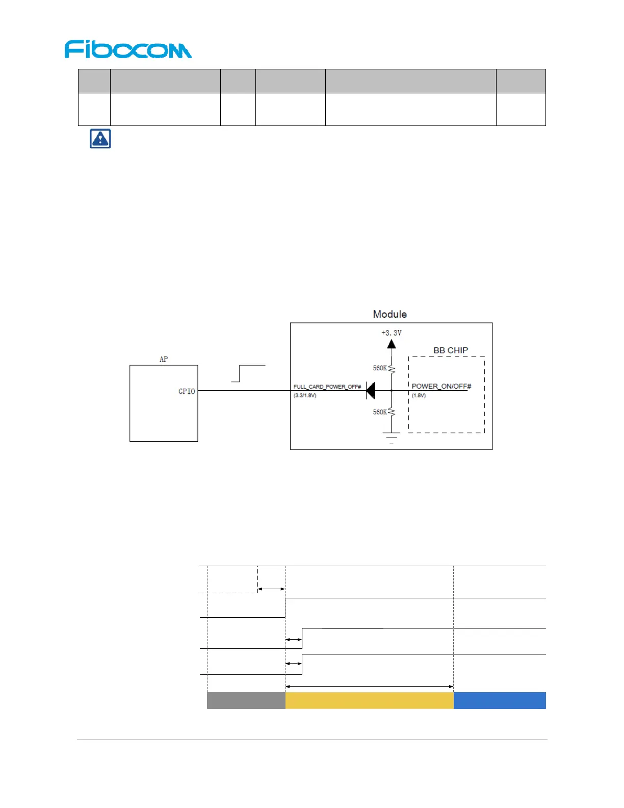
The FULL_CARD_POWER_OFF# pin needs an external 3.3V or 1.8V pull up for booting up. The
VDD_1V8 should be provided from the external circuit. AP (Application Processor) controls the module
start-up,and the circuit design is shown in Figure3-4:
Figure 3-4 Circuit for Module Start-up Controlled by AP
3.3.1.2 Start-up Timing Sequence
When power supply is ready, the PMU of module will power on and start initialization process by
pulling high FULL_CARD_POWER_OFF# signal. After about 10s, module will complete initialization
process. The start-up timing is shown in Figure 3-5:
+3.3V
PERST#
t
pr
RESET#
t
on
1
Module State
Initialization Activati on(AT Comma nd Ready)
FULL_CARD_POWER_OFF#
t
on
2
typical 10s
OFF
Figure 3-5 Timing Control for Start-up
 Loading...