Reproduction forbidden without Fibocom Wireless Inc. written authorization - All Rights Reserved.
L850-GL Hardware User Manual Page 18 of 54
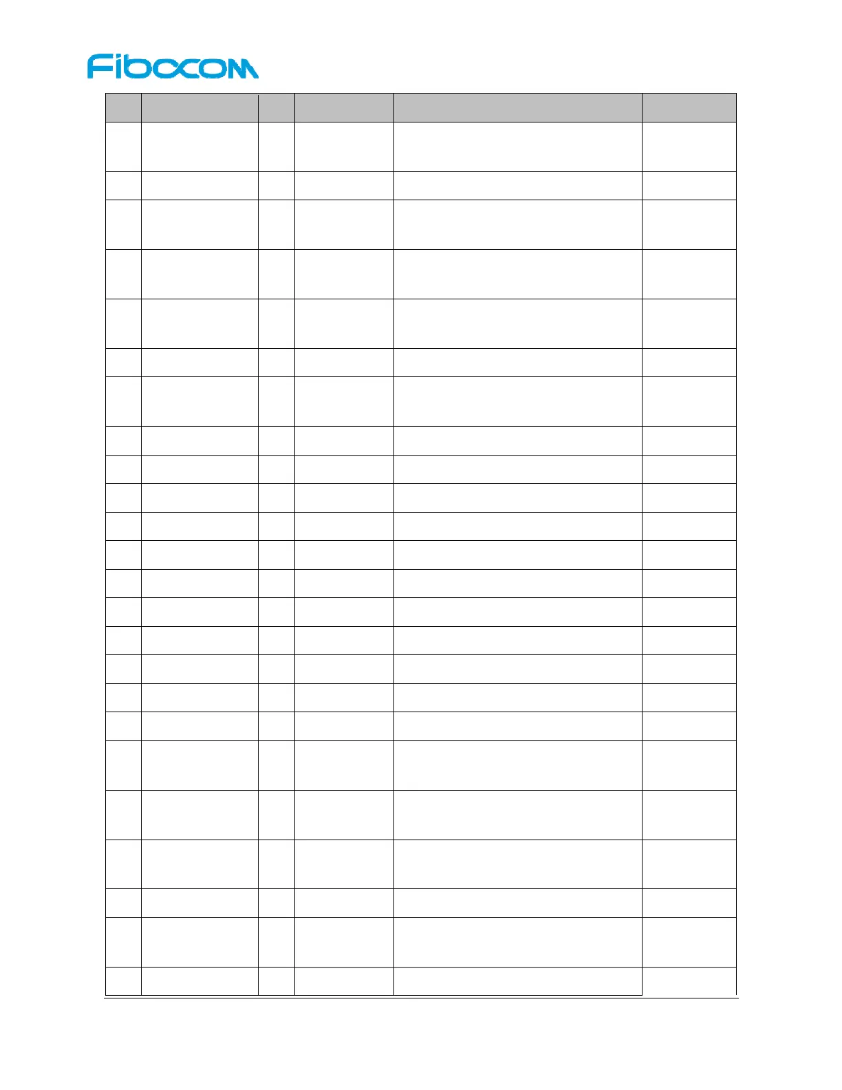
Pin Pin Name I/O Reset Value Pin Description Type
22 I2S_RX I PD
I2S Serial receive data,
Reserved
CMOS 1.8V
23 WOWWAN# O PD Wake up host
, Reserved
CMOS 1.8V
24 I2S_TX O PD
I2S Serial transmit data,
Reserved
CMOS 1.8V
25 DPR I PU Body SAR Detect, active low
CMOS
3.3/1.8V
26 W_DISABLE2# I PU
GNSS disable, active low,
Reserved
CMOS
3.3/1.8V
27 GND
GND Power Supply
28 I2S_WA O PD
I2S Word alignment/select,
Reserved
CMOS 1.8V
29
USB3.0_TX-
O
USB3.0 Transmit data minus
30
UIM_RESET
O
L
SIM reset signal
1.8V/3V
31
USB3.0_TX+
O
USB3.0 Transmit data plus
32
UIM_CLK
O
L
SIM clock Signal
1.8V/3V
33
GND
GND
电源
34
UIM_DATA
I/O
L
SIM data input/output
1.8V/3V
35
USB3.0_RX-
I
USB3.0 receive data minus
36
UIM_PWR
O
SIM power supply, 3V/1.8V
1.8V/3V
37
USB3.0_RX+
I
USB3.0 receive data plus
38 NC
NC
39 GND
GND Power Supply
40 GNSS_SCL O PU
I2C Serial clock,
Reserved
CMOS 1.8V
41 PETn0 O
PCIe TX Differential signals
Negative
42 GNSS_SDA I/O PU
I2C Serial data input/output,
Reserved
CMOS 1.8V
43 PETp0 O
PCIe TX Differential signals Positive
44 GNSS_IRQ I PD
GNSS Interrupt Request,
Reserved
CMOS 1.8V
45 GND
GND Power Supply
 Loading...