Reproduction forbidden without Fibocom Wireless Inc. written authorization - All Rights Reserved.
L850-GL Hardware User Manual Page 17 of 54
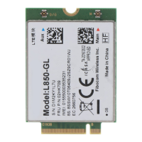
Pin “Notch” represents the gap of the gold fingers.
3.1.2 Pin Definition
The pin definition is as follows:
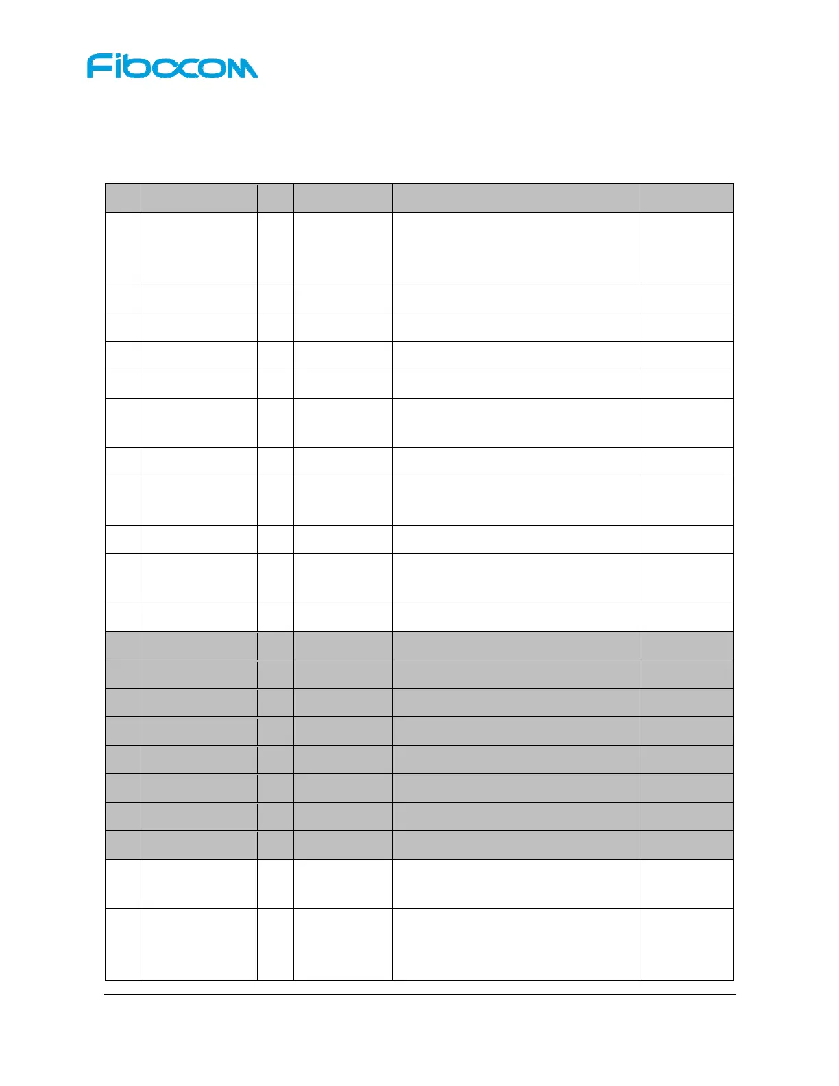
Pin Pin Name I/O Reset Value Pin Description Type
1 CONFIG_3 O
NC
NC, L850 M.2 module is configured as
the WWAN – PCIe, USB3.0 interface
type
2 +3.3V PI
Power input Power Supply
3 GND
GND Power Supply
4 +3.3V PI
Power input Power Supply
5 GND
GND Power Supply
6
FULL_CARD_
POWER_OFF#
I PU
Power enable, Module power on input,
internal pull up
CMOS
3.3/1.8V
7 USB D+ I/O
USB Data Plus 0.3---3V
8 W_DISABLE1# I PD WWAN Disable, active low
CMOS
3.3/1.8V
9 USB D- I/O
USB Data Minus 0.3---3V
10 LED1# O T
System status LED, Output open drain,
CMOS 3.3V
CMOS 3.3V
11 GND
GND Power Supply
12 Notch
Notch
13 Notch
Notch
14 Notch
Notch
15 Notch
Notch
16 Notch
Notch
17 Notch
Notch
18 Notch
Notch
19 Notch
Notch
20 I2S_CLK O PD
I2S Serial clock,
Reserved
CMOS 1.8V
21 CONFIG_0
GND
GND, L850 M.2 module is configured as
the WWAN – PCIe, USB3.0 interface
type


 To Next Page