Reproduction forbidden without Fibocom Wireless Inc. written authorization - All Rights Reserved.
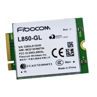
FIBOCOM L850-GL Series Hardware Guide Page 19 of 59
Pin Pin Name I/O Reset Value Pin Description Type
59 ANTCTL0 O
-
Tunable ANT CTRL0, bit0 1.8V
60 COEX3 I/O PD
Wireless coexistence between WWAN
and WiFi/BT modules, based on BT-
SIG
coexistence protocol. COEX_EXT_FTA,
Reserved
1.8V
61 ANTCTL1 O
-
Tunable ANT CTRL1, bit1 1.8V
62 COEX_RXD I T
Wireless coexistence between WWAN
and WiFi/BT modules, based on BT-
coexistence protocol. UART receive
signal(WWAN module side)
Reserved
1.8V
63 ANTCTL2 O
-
Tunable ANT CTRL2, bit2 1.8V
64 COEX_TXD O T
Wireless coexistence between WWAN
and WiFi/BT modules, based on BT-
coexistence protocol. UART transmit
signal(WWAN module side), Reserved
1.8V
65 NC -
-
NC -
66 SIM_DETECT I PD
SIM detect, internal pull up(390KΩ),
active high
1.8V
67 RESET# I -
WWAN reset input, internal pull
up(10KΩ), active low
1.8V
68 NC -
-
NC
-
69 CONFIG_1 O
GND
GND,
L850 M.2 module is configured as
the WWAN – PCIe, USB3.1 interface
type
-
70 +3.3V PI
-
Power input Power Supply
71 GND
- -
GND Power Supply
72 +3.3V PI
-
Power input Power Supply
73 GND
- -
GND Power Supply
74 +3.3V PI
-
Power input Power Supply
75 CONFIG_2 O
GND
GND, L850 M.2 module is configured as
the WWAN – PCIe, USB3.1 interface
type
-
 Loading...