EasyManuals Logo

Freenove Ultimate Starter Kit User Manual

Freenove Ultimate Starter Kit
286 pages
To Next Page IconTo Next Page
To Previous Page IconTo Previous Page
Page #102 background imageLoading...
Page #102 background image
Chapter 7 AD/DA Converter
102
www.freenove.com
support@freenove.com
PCF8591
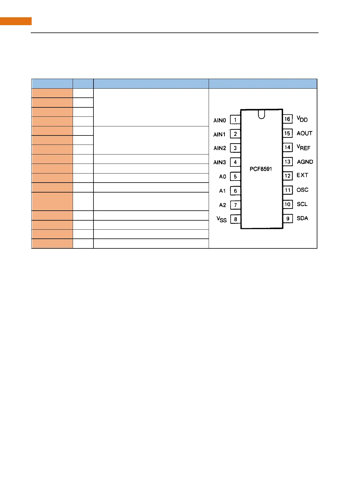
The PCF8591 is a single-chip, single-supply low power 8-bit CMOS data acquisition device with four analog
inputs, one analog output and a serial I2C-bus interface. The following table is the pin definition diagram of
PCF8591.
SYMBOL
PIN
DESCRIPTION
TOP VIEW
AIN0
1
Analog inputs (A/D converter)
AIN1
2
AIN2
3
AIN3
4
A0
5
Hardware address
A1
6
A2
7
Vss
8
Negative supply voltage
SDA
9
I2C-bus data input/output
SCL
10
I2C-bus clock input
OSC
11
Oscillator input/output
EXT
12
external/internal switch for oscillator
input
AGND
13
Analog ground
Vref
14
Voltage reference input
AOUT
15
Analog output(D/A converter)
Vdd
16
Positive supply voltage
For more details about PCF8591, please refer to datasheet.
I2C communication
I2C(Inter-Integrated Circuit) is a two-wire serial communication mode, which can be used to connection of
micro controller and its peripheral equipment. Devices using I2C communication must be connected to the
serial data (SDA) line, and serial clock (SCL) line (called I2C bus). Each device has a unique address and can be
used as a transmitter or receiver to communicate with devices connected to the bus.

Table of Contents

Questions and Answers:

Question and Answer IconNeed help?

Do you have a question about the Freenove Ultimate Starter Kit and is the answer not in the manual?

Freenove Ultimate Starter Kit Specifications

General IconGeneral
BrandFreenove
ModelUltimate Starter Kit
CategorySingle board computers
LanguageEnglish