GE Multilin F35 Multiple Feeder Protection System B-39
APPENDIX B B.4 MEMORY MAPPING
B
IEC 61850 Server Configuration (Read/Write Settings/Commands)
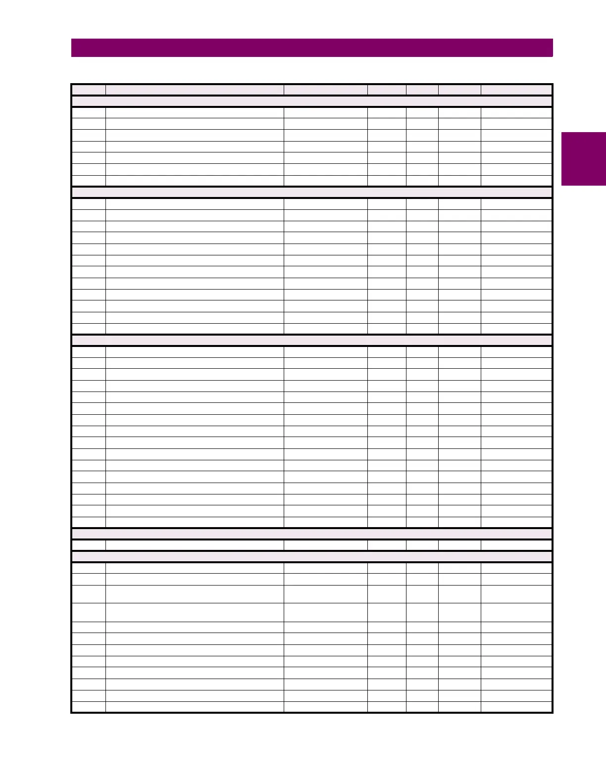
AAD0 TCP Port Number for the IEC 61850 / MMS Protocol 1 to 65535 --- 1 F001 102
AAD1 IEC 61850 Logical Device Name --- --- --- F213 “IECName”
AAE1 IEC 61850 Logical Device Instance --- --- --- F213 “LDInst”
AAF1 IEC 61850 LPHD Location --- --- --- F204 “Location”
AB19 Include non-IEC 61850 Data 0 to 1 --- 1 F102 0 (Disabled)
AB1A IEC 61850 Server Data Scanning Function 0 to 1 --- 1 F102 0 (Disabled)
AB1B Reserved (15 items)
IEC 61850 XCBR configuration (read/write settings)
AB24 Operand for IEC 61850 XCBR1.ST.Loc status 0 to 65535 --- 1 F300 0
AB25 Command to clear XCBR1 OpCnt (operation counter) 0 to 1 --- 1 F126 0 (No)
AB26 Operand for IEC 61850 XCBR2.ST.Loc status 0 to 65535 --- 1 F300 0
AB27 Command to clear XCBR2 OpCnt (operation counter) 0 to 1 --- 1 F126 0 (No)
AB28 Operand for IEC 61850 XCBR3.ST.Loc status 0 to 65535 --- 1 F300 0
AB29 Command to clear XCBR3 OpCnt (operation counter) 0 to 1 --- 1 F126 0 (No)
AB2A Operand for IEC 61850 XCBR4.ST.Loc status 0 to 65535 --- 1 F300 0
AB2B Command to clear XCBR4 OpCnt (operation counter) 0 to 1 --- 1 F126 0 (No)
AB2C Operand for IEC 61850 XCBR5.ST.Loc status 0 to 65535 --- 1 F300 0
AB2D Command to clear XCBR5 OpCnt (operation counter) 0 to 1 --- 1 F126 0 (No)
AB2E Operand for IEC 61850 XCBR6.ST.Loc status 0 to 65535 --- 1 F300 0
AB2F Command to clear XCBR6 OpCnt (operation counter) 0 to 1 --- 1 F126 0 (No)
IEC 61850 LN name prefixes (read/write settings)
AB30 IEC 61850 logical node LPHD1 name prefix 0 to 65534 --- 1 F206 (none)
AB33 IEC 61850 logical node PIOCx name prefix (72 items) 0 to 65534 --- 1 F206 (none)
AC0B IEC 61850 logical node PTOCx name prefix (24 items) 0 to 65534 --- 1 F206 (none)
AC53 IEC 61850 logical node PTUVx name prefix (13 items) 0 to 65534 --- 1 F206 (none)
AC7A IEC 61850 logical node PTOVx name prefix (10 items) 0 to 65534 --- 1 F206 (none)
AC98 IEC 61850 logical node PDISx name prefix (10 items) 0 to 65534 --- 1 F206 (none)
ACB6 IEC 61850 logical node RBRFx name prefix (24 items) 0 to 65534 --- 1 F206 (none)
ACFE IEC 61850 logical node RPSBx name prefix 0 to 65534 --- 1 F206 (none)
AD01 IEC 61850 logical node RRECx name prefix (6 items) 0 to 65534 --- 1 F206 (none)
AD13 IEC 61850 logical node MMXUx name prefix (6 items) 0 to 65534 --- 1 F206 (none)
AD25 IEC 61850 logical node GGIOx name prefix (4 items) 0 to 65534 --- 1 F206 (none)
AD31 IEC 61850 logical node RFLOx name prefix (5 items) 0 to 65534 --- 1 F206 (none)
AD40 IEC 61850 logical node XCBRx name prefix (6 items) 0 to 65534 --- 1 F206 (none)
AD52 IEC 61850 logical node PTRCx name prefix (6 items) 0 to 65534 --- 1 F206 (none)
AD64 IEC 61850 logical node PDIFx name prefix (6 items) 0 to 65534 --- 1 F206 (none)
AD70 IEC 61850 logical node MMXNx name prefix (6 items) 0 to 65534 --- 1 F206 (none)
IEC 61850 GGIO4 general analog configuration settings (read/write)
AF00 Number of analog points in GGIO4 4 to 32 --- 4 F001 4
IEC 61850 GGIO4 analog input points configuration settings (read/write)
AF10 IEC 61850 GGIO4 analog input 1 value --- --- --- F600 0
AF11 IEC 61850 GGIO4 analog input 1 deadband 0.001 to 100 % 0.001 F003 100000
AF13 IEC 61850 GGIO4 analog input 1 minimum –1000000000000 to
1000000000000
--- 0.001 F060 0
AF15 IEC 61850 GGIO4 analog input 1 maximum –1000000000000 to
1000000000000
--- 0.001 F060 1000000
AF17 ...Repeated for IEC 61850 GGIO4 analog input 2
AF1E ...Repeated for IEC 61850 GGIO4 analog input 3
AF25 ...Repeated for IEC 61850 GGIO4 analog input 4
AF2C ...Repeated for IEC 61850 GGIO4 analog input 5
AF33 ...Repeated for IEC 61850 GGIO4 analog input 6
AF3A ...Repeated for IEC 61850 GGIO4 analog input 7
AF41 ...Repeated for IEC 61850 GGIO4 analog input 8
AF48 ...Repeated for IEC 61850 GGIO4 analog input 9
Table B–9: MODBUS MEMORY MAP (Sheet 32 of 48)
ADDR REGISTER NAME RANGE UNITS STEP FORMAT DEFAULT