Marquette Hellige GmbH MAC 1100/1200 V 1.1 Page 20
227 492 20 D - 0002
2.5.2 Electronic interfaces
This section describes the pinning, function and significance of the signals on the
internal interfaces of the functional components.
2.5.2.1 Interface to the switching power supply
The interface to the switching power supply is realized by the connector POSUP/ on
the PCB Control CS_CI.
Connector denotation: POSUP/
Type: male connector 1 X 4-pin., 180°, AMP MODU I
reverse terminal protection achieved mechanically.
The function of the individual pins is given in the following table . The definition as an
input/output is seen with reference to PCB Control CS_CI.
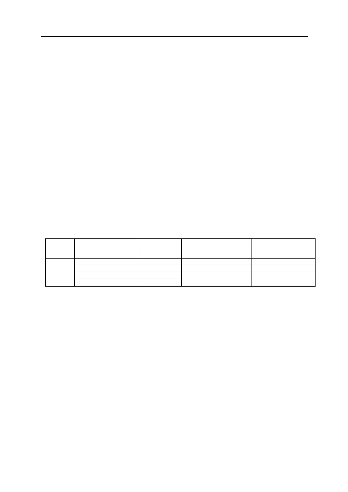
POSUP/
Pin
Number
Signal Name input/output Function Definition
1 +24VPS In
ut Volta
e from
ower su
.+ 26
5V
2 +24VPS Input Volta
e from power sup. + 26,5V
3 GNDPS Input GND from power suppl
4 GNDPS Input GND from power suppl
2.5.2.2 Interface to the PCB NC battery charge
This interface has the supply for battery charging, charging control and status
signals and the battery voltage from the PCB NC battery charge.
Connector denotation: BATT/
Type: male multipoint connector 2x 10-pin, 180°
reverse terminal protection and coding with coding pin 15
The function of the individual pins is given in the following table . The definition as an
input/output is seen with reference to PCB Control CS_CI.
 Loading...