A change in VOX delay after operating for a period of time can be caused by leakage in diode D201. The
other possibility is a change in value of capacitor C213. Either component could experience a change in
operation characteristics due to heat.
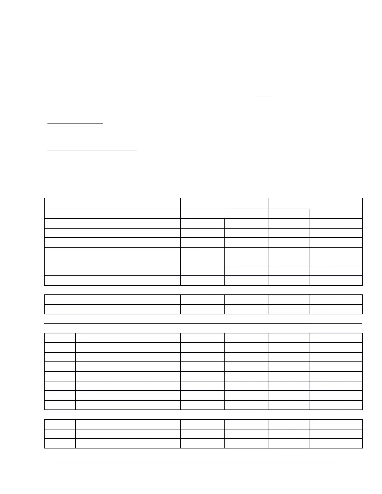
v.2.2. Transmit RF Signal Levels
The transmit levels listed are based on measurements taken on two SB-102 radios and
are intended to provide a general ball-park figure rather than any kind of specification.
Test Setup SB-102
Remove 6146 Screen voltage by removing MOLEX plug on rear - easier on finals. TUNE mode, Peak
the DRIVER/PRESELECTOR for maximum drive.
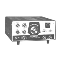
Test Setup SB-101 & HW-101
Remove 6146 Screen voltage by disconnecting R920 (100 ohm to Pin 3 on 6146s) - easier on finals.
TUNE mode, Peak the DRIVER/PRESELECTOR for maximum drive.
RF Volts measured with Heathkit VTVM & RF Probe. Scope measured with wideband scope using 10x
probe
Oscillators Volts (RF Probe) Volts (Scope, Peak-to-Peak)
Reference Actual Reference Actual
V16 Pin 3 or 8 (Carrier Oscillator) LSB 2.00 5.66
V16 Pin 3 or 8 (Carrier Oscillator) USB 2.00 5.66
Carrier Balance Pot. (center) 1.50 4.24
V19 Pin 2 (Het Osc. Cathode Follower
Grid)
5.00 14.14
V19 Pin 3 (Het Osc. Cathode Follower) 2.00 5.66
V5 Pin 7 or V12 Pin 7 (VFO)/LMO) 2.00 5.66
V5 Pin 2 (1st TX Mixer Grid) 2.20 6.22
V6 Pin 1 (2nd TX Mixer Grid) 1.20 3.39
V7 Pin 1 (Driver Grid) - Peak Driver/Preselector control for maximum voltage
3.5 3,700 KHz 3.00 8.48
7.0 7,200 KHz 2.60 7.35
14.0 14,200 KHz 3.30 9.33
21.0 21,200 KHz 3.50 9.90
28.0 28,200 KHz 2.40 6.79
28.5 28,700 KHz 2.40 6.79
29.0 29,200 KHz 2.40 6.79
29.5 29,700 KHz 2.40 6.79
Driver Out Jack on Rear Panel (SB-102 only) - Peak Driver/Preselector control for maximum voltage
3.5 3,700 KHz 3.5 9.90
7.0 7,200 KHz 3.75 10.61
14.0 14,200 KHz 3.80 10.75
Signal Level Measurements Page 50