71
2.9 Basic Timing
2.9.1 Overview
The H8S/2600 CPU is driven by a system clock, denoted by the symbol ø. The period from one
rising edge of ø to the next is referred to as a "state." The memory cycle or bus cycle consists of
one, two, or three states. Different methods are used to access on-chip memory, on-chip
supporting modules, and the external address space.
2.9.2 On-Chip Memory (ROM, RAM)
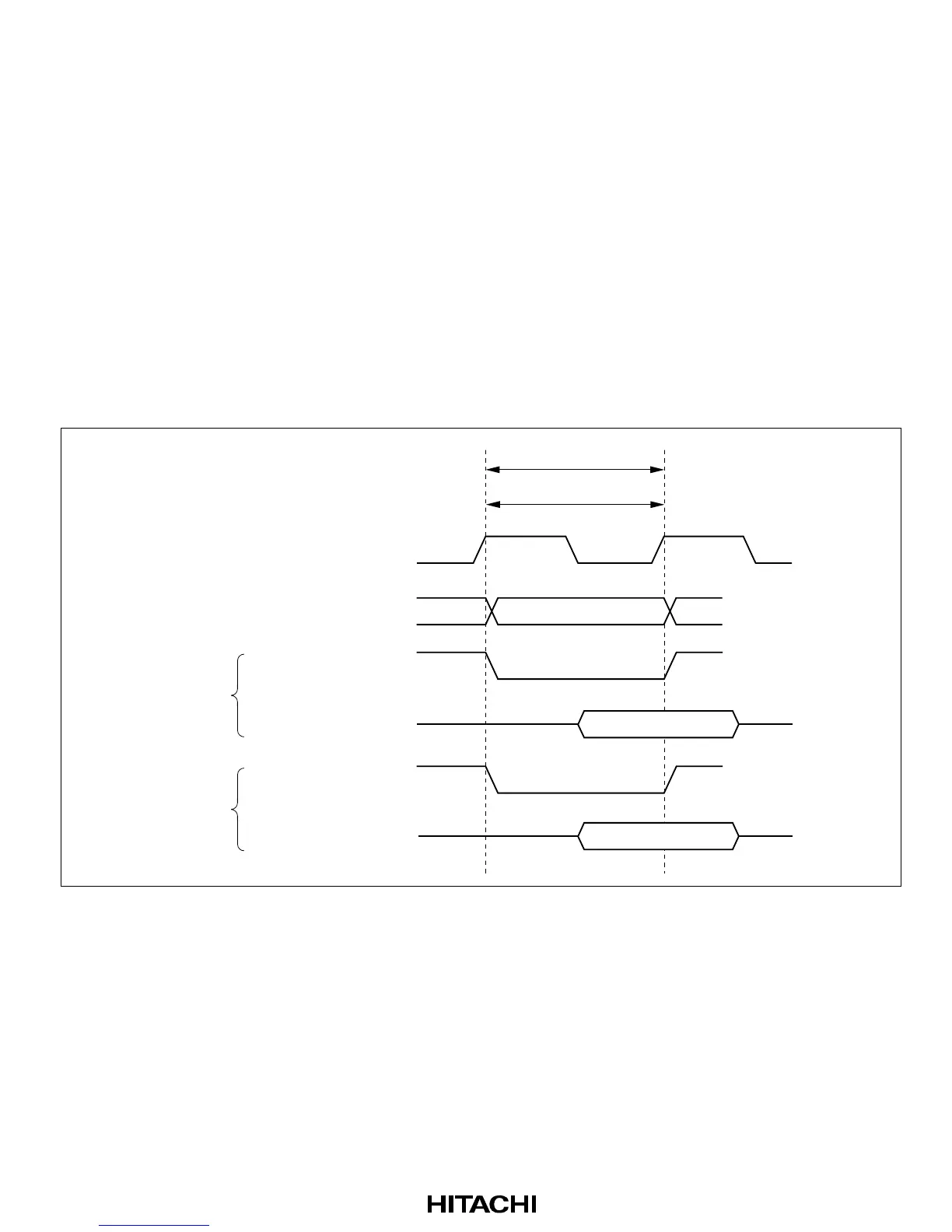
On-chip memory is accessed in one state. The data bus is 16 bits wide, permitting both byte and
word transfer instruction. Figure 2-17 shows the on-chip memory access cycle. Figure 2-18 shows
the pin states.
Internal address bus
Internal read signal
Internal data bus
Internal write signal
Internal data bus
ø
Bus cycle
T1
Address
Read data
Write data
Read
access
Write
access
Figure 2-17 On-Chip Memory Access Cycle
 Loading...