696
Table 20-9 Programmer Mode Pin Settings
Pin Names Settings
Mode pins: MD2, MD1, MD0 Low level input to MD2, MD1, and MD0.
Mode setting pins: PF0, P16, P14 High level input to PF0, low level input to P16 and P14
FWE pin High level input (in auto-program and auto-erase
modes)
RES pin Reset circuit
XTAL, EXTAL, PLLCAP, PLLV
SS
pins Oscillator circuit
VCL Internal step-down circuit
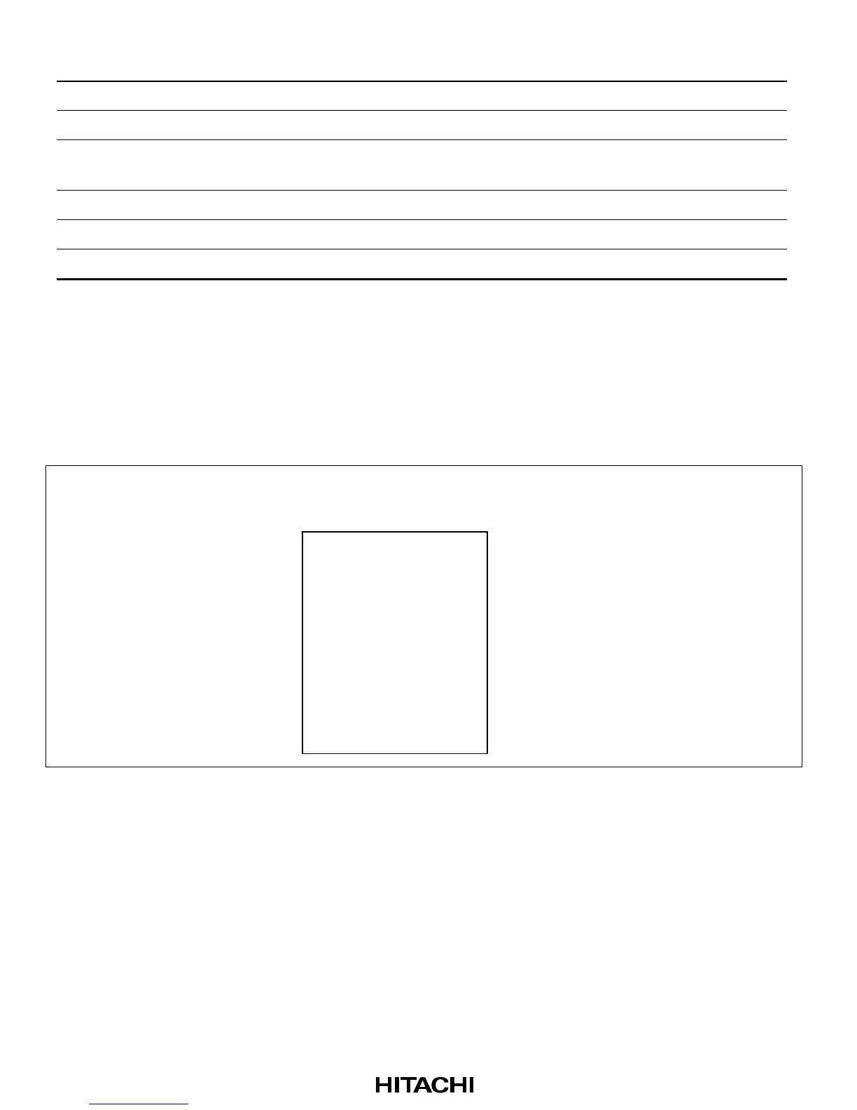
20.11.1 Socket Adapter Pin Correspondence Diagram
Connect the socket adapter to the chip as shown in figure 20-17. This will enable conversion to a
40-pin arrangement. The on-chip ROM memory map is shown in figure 20-16, and the socket
adapter pin correspondence diagram in figure 20-17.
H'000000
Addresses in
MCU mode
Addresses in
programmer mode
H'01FFFF
H'00000
H'1FFFF
On-chip ROM space
128 kbytes
Figure 20-16 On-Chip ROM Memory Map
 Loading...