603
Table 16-4 A/D Conversion Time (Single Mode)
CKS1 = 0 CKS1 = 0
CKS0 = 0 CKS0 = 1 CKS0 = 0 CKS0 = 1
Item Symbol Min Typ Max Min Typ Max Min Typ Max Min Typ Max
A/D conversion start delay t
D
18 — 33 10 — 17 6 — 9 4 — 5
Input sampling time t
SPL
— 127 — — 63 — — 31 — — 15 —
A/D conversion time t
CONV
55 — 530 259 — 266 131 — 134 67 — 68
Note: Values in the table are the number of states.
Table 16-5 A/D Conversion Time (Scan Mode)
CKS1 CKS0 Conversion Time (State)
0 0 512 (Fixed)
1 256 (Fixed)
1 0 128 (Fixed)
1 64 (Fixed)
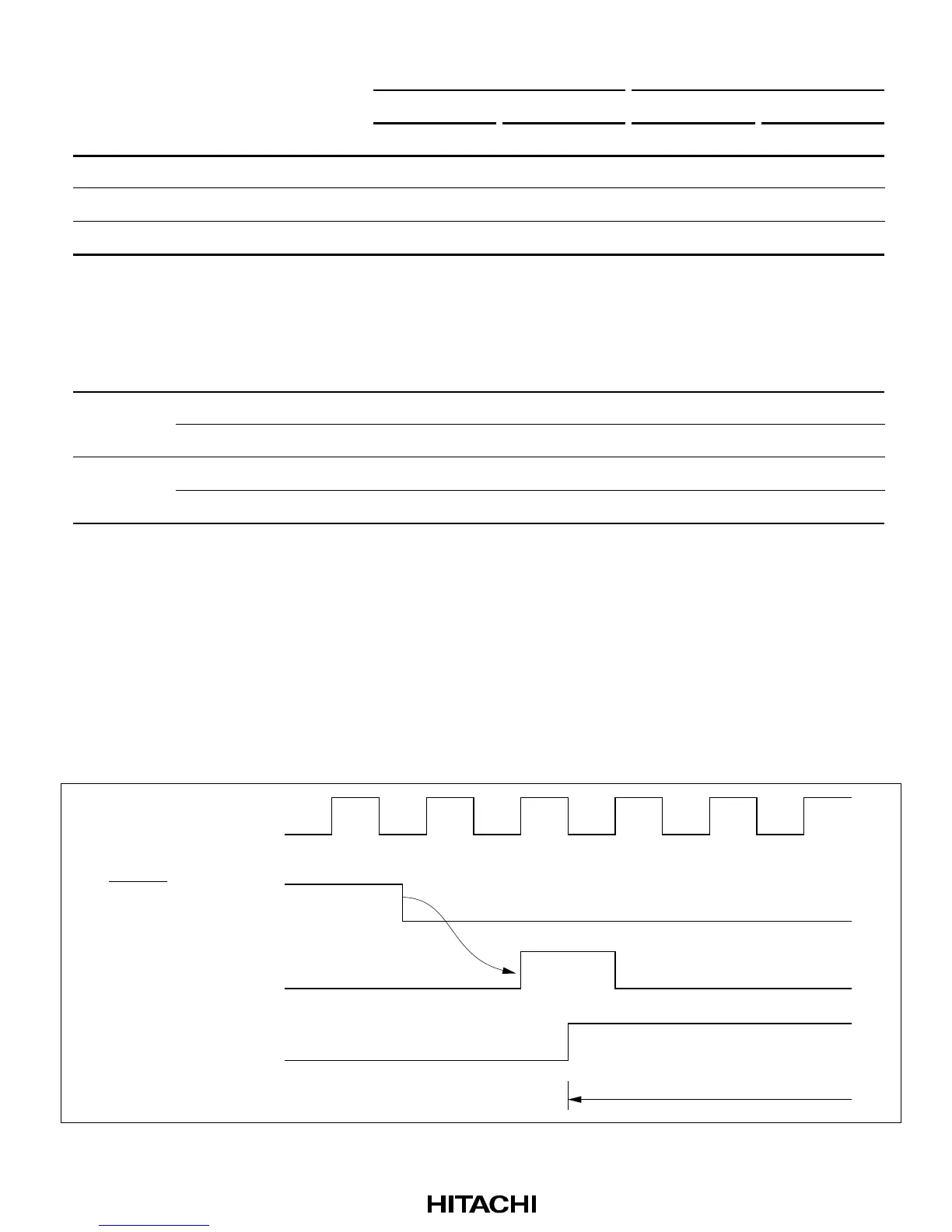
16.4.4 External Trigger Input Timing
A/D conversion can be externally triggered. When the TRGS1 and TRGS0 bits are set to 11 in
ADCR, external trigger input is enabled at the ADTRG pin. A falling edge at the ADTRG pin sets
the ADST bit to 1 in ADCSR, starting A/D conversion. Other operations, in both single and scan
modes, are the same as if the ADST bit has been set to 1 by software. Figure 16-6 shows the
timing.
ø
ADTRG
Internal trigger signal
ADST
A/D conversion
Figure 16-6 External Trigger Input Timing
 Loading...