652
Table 18-4 Power-Down Modes and Display Operation
Mode Reset Active Sleep Watch Subactive Subsleep Standby
Module
Standby
Clock ø Runs Runs Runs Stops Stops Stops Stops Stops
*4
ø
SUB
Runs Runs Runs Runs Runs Runs Stops
*1
Stops
*4
Display ACT = 0 Stops Stops Stops Stops Stops Stops Stops
*2
Stops
operation
ACT = 1 Stops Functions Functions Functions
*3
Functions
*3
Functions
*3
Stops
*2
Stops
Notes: *1 The subclock oscillator does not stop, but clock supply is halted.
*2 The LCD drive power supply is turned off regardless of the setting of the PSW bit.
*3 Display operation is performed only if ø
SUB
, ø
SUB
/2, or ø
SUB
/4 is selected as the operating
clock.
*4 The clock supplied to the LCD stops.
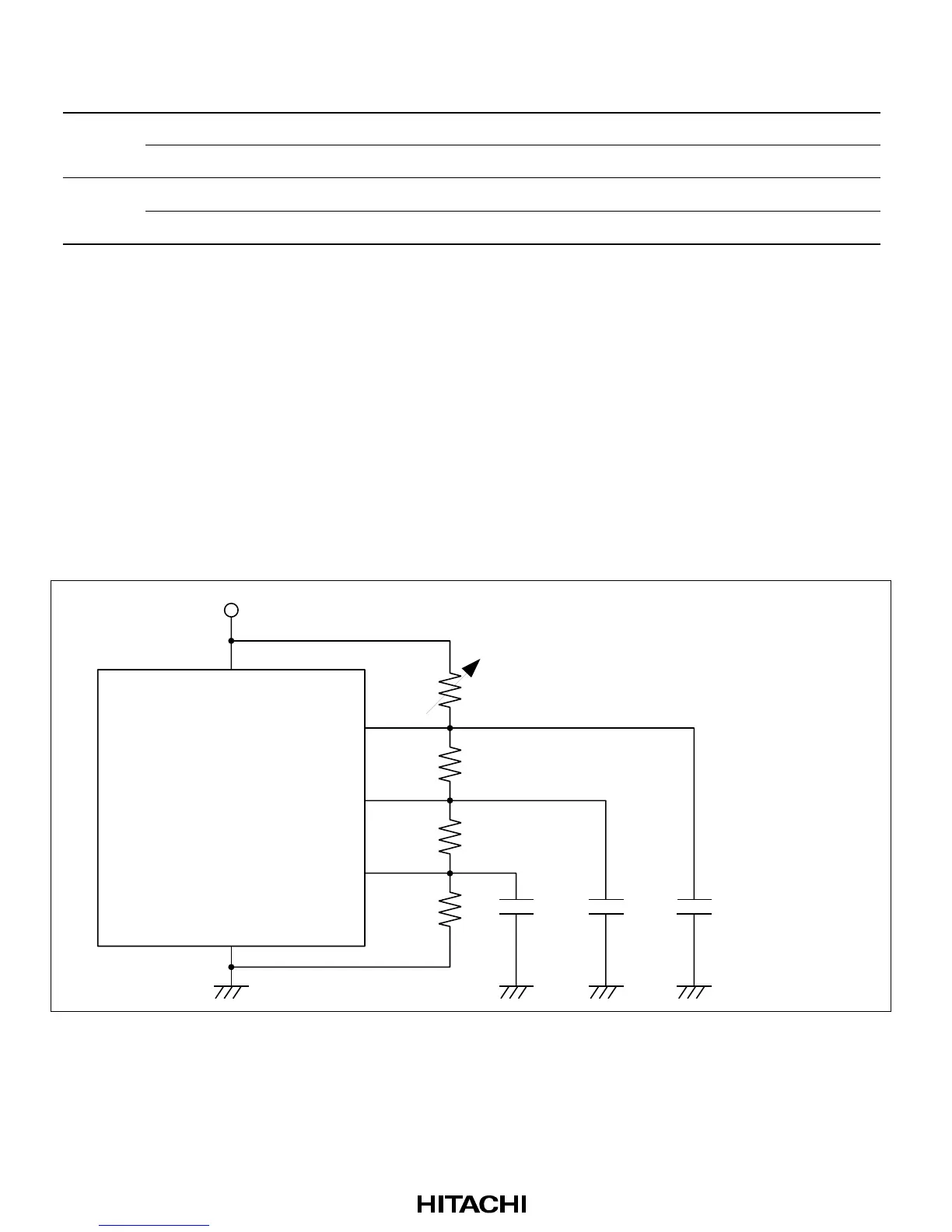
18.3.4 Boosting the LCD Drive Power Supply
When a panel is driven, the on-chip power supply capacity may be insufficient. The recommended
solution in this case is to connect bypass capacitors of around 0.1 to 0.3 µF to pins V1 to V3, or to
connect a new split-resistance externally, as shown in figure 18-13.
H8S/2646 Series
LPV
CC
V
SS
V1
V2
V3
VR
R
R
R
R =
C = 0.1 to 0.3 µF
several kΩ to
several MΩ
Figure 18-13 Connection of External Split-Resistance
 Loading...