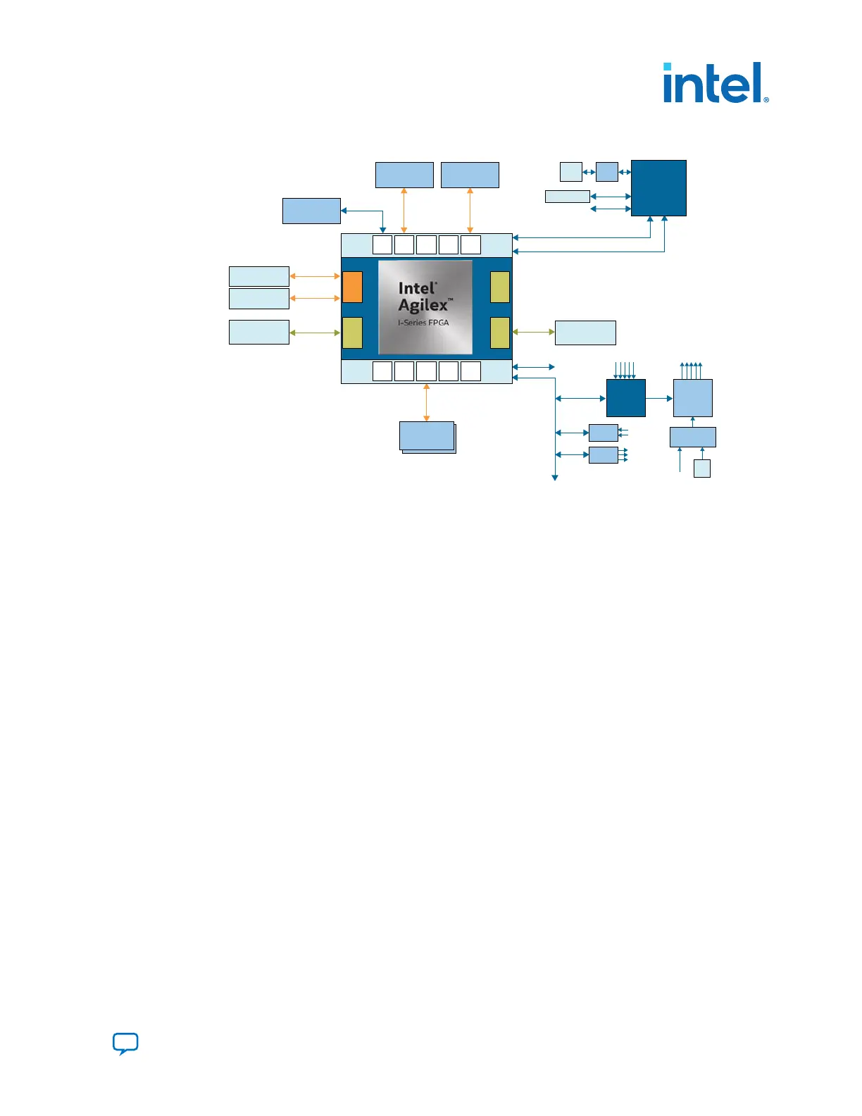
Figure 1. Intel Agilex I-Series FPGA Development Kit Board Diagram
x16
28G/56Gx8
28G/56Gx8
x72
AVST x8
x72
Dual x8
GPIO
x72, 2-DPC
I
2
C
Temp
Diodes
All Voltages
Voltage Sense
Inputs
All Clocks
Seq Ctrl
GPIOs,
Push-buttons,
LEDs
Intel MAX 10
FPGA
Power Seq.
Power
Monitor
JTAG
JTAG Header
I
2
C
I/Os
JTAG
Aux 12V
Conn
+12V from
PCIe Gold
Fingers
Dual DIMM
DDR4 / DDR-T
15A
R-Tile
x16
15C
R-Tile
x16
14C
R-Tile
x16
CXL/PCIe Gen 5 x16
Edge Conn
QSFPDD -2
QSFPDD -1
USB
Conn
CXL/PCIe Connector
x2 MCIO
Aux
12V
SDM 2B 2E 2F 2C
Temp
Sense
Power
Regulators
Hot-Plug and
PWR or CKT
Clocks
Intel® MAX® 10
FPGA
Intel FPGA
Download Cable II
JTAG SW
I
2
C CTRL
Config QSPI
2 Gb Flash
Comp -CH0
DDR4 x72 with ECC
Comp -CH1
DDR4 x72 with ECC
12A
F-Tile
x20
GPIO
3A 3B 3C 3D HPS
USB
PHY
Feature Summary
• Intel Agilex I-Series (AGIB027) device in the 2957A BGA package
— 0.8 VID-adjustable VCC core
— R-tile transceivers supporting PCIe Gen5/CXL
(1)
— F-tile transceivers supporting 56 Gbps NRZ
• FPGA configuration
— Partial reconfiguration support
— Configuration via Protocol (CvP) configuration support
— 2 Gb QSPI flash
— Storage for two configuration images in flash (factory and user)
— JTAG header for device programming
— Built-in Intel FPGA Download Cable II for device programming
• Programmable clock sources
— 156.25 MHz differential LVDS for F-tile (QSFPDD)
— 100.000 MHz HCSL for PCIe and CXL (R-tile)
— 33.33 MHz differential LVDS for memory
— 125 MHz configuration clock
— 100 MHz differential LVDS for I/O banks
1. Overview
683288 | 2022.09.22
Send Feedback
Intel
®
Agilex
™
I-Series FPGA Development Kit User Guide
5

 Loading...


