EasyManua.ls Logo

JVC AX-Z1010TN - User Manual

JVC AX-Z1010TN
67 pages
Print Icon
To Next Page IconTo Next Page
Loading...
AX-Z1010TN
JVC
SERVICE
MANUAL
Contents
Safety
Precautions
..........ccccceecceecesseeteneeeneseenees
1-2
Specifications
Operating
Instructions..
Description
of
Technology
.
Removal
Procedures........
+
1-20
Adjustment
Procedures
Description
of
Major
ICs..
Internal
Block
Diagrams
of
Other
ICs................
1-30
Block
Diagram
..
Insertion
Schematic
Diagrams...
.
Insertion
Connection
Diagram
..
Insertion
Printed
Circuit
Boards
.
..
Insertion
Parts
List..
.
Separate
Volume
Insertion
No.
20115,
Jun
1989
Question and Answer IconNeed help?

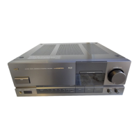
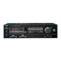
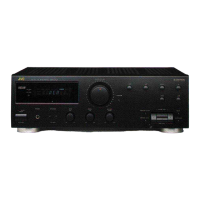
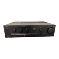
Do you have a question about the JVC AX-Z1010TN and is the answer not in the manual?

JVC AX-Z1010TN Specifications

General IconGeneral
BrandJVC
ModelAX-Z1010TN
CategoryAmplifier
LanguageEnglish

Summary

Safety Precautions

Warning

Essential safety guidelines for equipment repair and operation.

Specifications

Connection Diagram

Front Panel

How to Operate

Digital Pure A TYPE II

COMPU LINK Remote Control System

Description of COMPU LINK system features like automatic source selection and synchronized recording.

Remote Control Unit (RM-SA1010 U)

Description and Functions

Details on remote control unit buttons, including source selection and volume controls.

Using S.E.A. Graphic Equalizer;Processor

Connecting to SEA

Instructions for connecting and using an SEA graphic equalizer.

Connecting to Processors

Connecting to a JVCs DAP

Guidance on connecting a Digital Acoustics Processor (DAP) to the unit.

Troubleshooting

Description of Technology

Digital Pure-A

Explanation of the Digital Pure-A operation system based on signal prediction.

Prediction Signal Generation Circuit

Details on the circuit that generates prediction signals for amplifier operation.

Removal Procedures

Removing the Top Cover

Steps to remove the top cover of the unit.

Removing the Front Panel

Steps to detach and remove the front panel.

Removing the Front PC Board and the Key Input PC Board

Procedure for removing the front PC board and key input board.

Disconnecting the Protector PC Board

Steps to disconnect and remove the protector PC board.

Disconnecting the Power Supply PC Board and Removing the Sub Heat Sink

Instructions for disconnecting the power supply board and removing the heat sink.

Removing the DAC PC Board

Steps to remove the DAC PC board.

Disconnecting the Analog Input PC Board

Steps to disconnect and remove the analog input PC board.

Disconnecting the Motor Control Input Board

Procedure for disconnecting the motor control input board.

Disconnecting the Power Amplifier PC Board and the Power Transistors

Instructions for disconnecting the power amplifier board and transistors.

Disconnecting the Relay PC Board

Steps to disconnect and remove the relay PC board.

Adjustment Procedures

Power Amplifier Adjustment (Idling Adjustment)

Procedure for adjusting the power amplifier's idling current.

Description of Major ICs

Optical Receiving Module (TORX172)

Technical description and circuit configuration of the optical receiving module.

Digital Audio Interface Receiver (YM3623 B)

Overview of the YM3623B's functions in digital audio interface reception.

K2 Interface and Delay Circuit (VC4111)

Description of the VC4111 IC, its appearance and pin functions.

Octuple Oversampling Digital Filter (YM3414)

Description of the YM3414 IC, its appearance and block diagram.

System Control Microcomputer (µPD75104 CW-150)

Description of the µPD75104CW-150 IC, including its functions and pin layout.

Static RAM (LC3517 BSL-15)

Description of the LC3517BSL-15 Static RAM IC.

D;A Converters (PCM56 P)

Description of the PCM56P ICs used as D/A converters.

Voltage Controlled Oscillator (SN74 LS624 N)

Description of the SN74LS624N IC used as a Voltage Controlled Oscillator.

Motor Driver (LB1639-CV)

Description of the LB1639-CV IC used as a motor driver.

Super-A ICs (VC5022-2)

Description of the VC5022-2 ICs related to Super-A amplifier technology.

Protector (µPC1237 HA)

Description of the µPC1237HA IC used for circuit protection.

CMOS Logic ICs (TC74 HC series)

Descriptions of various CMOS logic ICs, including inverters, NAND, OR gates, and flip-flops.

Phase Detector for PLL (TC5081 AP)

Description of the TC5081AP IC used as a phase detector for PLL.

Parts List

Exploded Views and Parts List

Visual breakdown of unit components with corresponding part numbers.

Printed Circuit Board Assy and Parts List

Details on various printed circuit boards and their associated parts.

Packing Materials and Part Numbers

Information on packaging materials and part identification codes.

Accessories List

List of included accessories with their part numbers and descriptions.

Block Diagrams

Digital Signal Processing Circuit

Block diagram illustrating the digital signal processing path.

Analog Signal Processing Circuit

Block diagram showing the analog signal processing stages.

System Control Microprocessor Peripheral Circuit

Signal Prediction Circuit

Diagram of the circuit responsible for predicting signal behavior.

Bias Current Adjustment Circuit

Circuit diagram for adjusting bias current in the amplifier.

Schematic Diagrams

Power Primary Section

Schematic of the power supply and primary circuit components.

Connection Diagram

Printed Circuit Board Assy

Font & Analog Input PC Board (ENE-051)

Layout and component placement for the Analog Input PC Board.

Power Switch & AC Outlets PC Board (END-056)

Power Amplifier PC Board (ENH-120)

DAC & Power Supply PC Board (ENP-014)

Exploded Views and Parts List

Packing Materials and Part Numbers

Accessories List

Schematic Diagrams

Power Supply and System Control Section

Detailed schematic of power supply and system control circuits.

Schematic Diagrams

Source Input and Power Amplifier Section

Schematic detailing input sources and the power amplifier stage.

Related product manuals