Figure 2-3 provides a block diagram of the analog circuitry. Table 2-17 is provided to show
where the various switching devices are located in the block diagram.
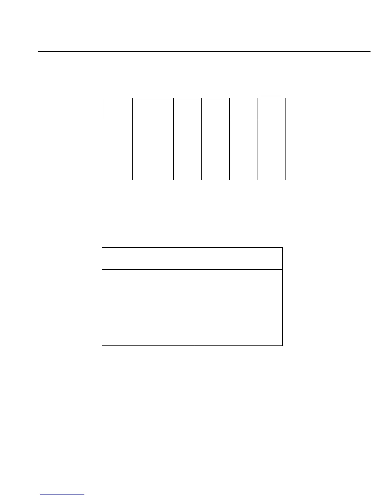
Table 2-16
Ω
4 signal multiplexing and gain
Range
Signal
(U163)
U129
pin 1
U129
pin 8
U129
pin 9
Gain
(U166)
100Ω
1kΩ
10kΩ
100kΩ
1MΩ
10MΩ
100MΩ
S4 then S7
S4 then S7
S4 then S7
S4 then S7
S4 then S7
S4 then S7
S4 then S7
OFF
OFF
OFF
OFF
ON
ON
ON
OFF
ON
ON
ON
OFF
OFF
OFF
ON
OFF
OFF
OFF
OFF
OFF
OFF
×100
×10
×10
×10
×1
×1
×1
Table 2-17
Circuit section locations for switching devices
Switching devices
Analog circuit section
(see Figure 2-3)
Q101, Q102
Q114, Q136, Q109
K101, Q113, Q105, Q104, Q108
Q121
K102, U103, U105, U111
U133, Q123, Q125, Q124,
Q126, Q120
K103
U163, U129
SSP (Solid State Protection)
DCV Divider
DCV & Ohms Switching
Sense LO
AC Switching & Gain
Ohms I-Source
Current Shunts
A/D Mux & Gain
Troubleshooting 2-17