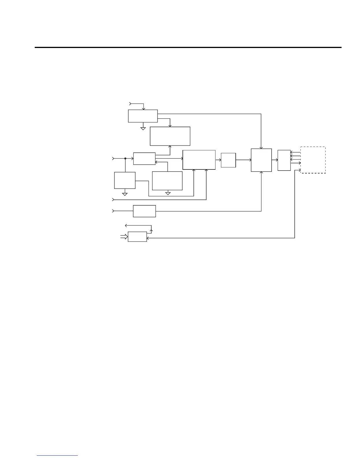
Analog circuitry
Refer to Figure 2-3 for the following discussion on analog circuitry.
INPUT HI
INPUT HI protection is provided by the SSP (solid state protection) circuit. The SSP is pri-
marily made up of Q101 and Q102. An overload condition opens Q101 and Q102. This discon-
nects the analog input signal from the rest of the analog circuit.
Note that for the 100VDC and 1000VDC ranges, Q101 and Q102 of the SSP are open. The
DC voltage signal is routed through the DCV Divider (Q114 and Q136 on) to the DCV switch-
ing circuit.
AMPS input
The ACA or DCA input signal is applied to the Current Shunt circuit, which is made up of
K103, R158 and R205. For the 10mADC range, 10.1
Ω
(R158 + R205) is shunted across the in-
put. Relay K103 is energized (on) to select the shunts. For all other DCA ranges, and all ACA
ranges, 0.1
Ω
(R158) is shunted across the input (K103 off).
The ACA signal is then sent to the AC Switching & Gain circuit, while the DCA signal is rout-
ed directly to the A/D MUX & Gain circuit.
Figure 2-3
Analog circuitry
block diagram
AMPS
Current
Shunts
K103, R158, R205
DCA
ACA
AC Switching
&
Gain
K102, U102, U103, U105,
U112, U118, U111, U110
ACV,
FREQ
INPUT
HI
SSP*
Q101, Q102
DCV
OHMS
DCV
Divider
R117, Q109,
Q114, Q136
Ohms I-Source
U133, Q123, Q125,
Q124, Q126, Q119,
Q120, U123
DCV/100
DCV & Ohms
Switching
K101, Q104, Q105,
Q108, Q113, U115
SENSE
HI
X1
Buffer
U113
BUFCOM
A/D
MUX &
Gain
U163, U166
U129, U132
ADC
U165
Digital
Circuitry
(See Figure 2-2)
SENSE
LO
X1 Buffer
Q121, U126
Scanner Output
Scanner
Inputs
Scanner
Option
Scanner Control
*Solid State Protection
Troubleshooting 2-9