DP990/DP995service manual
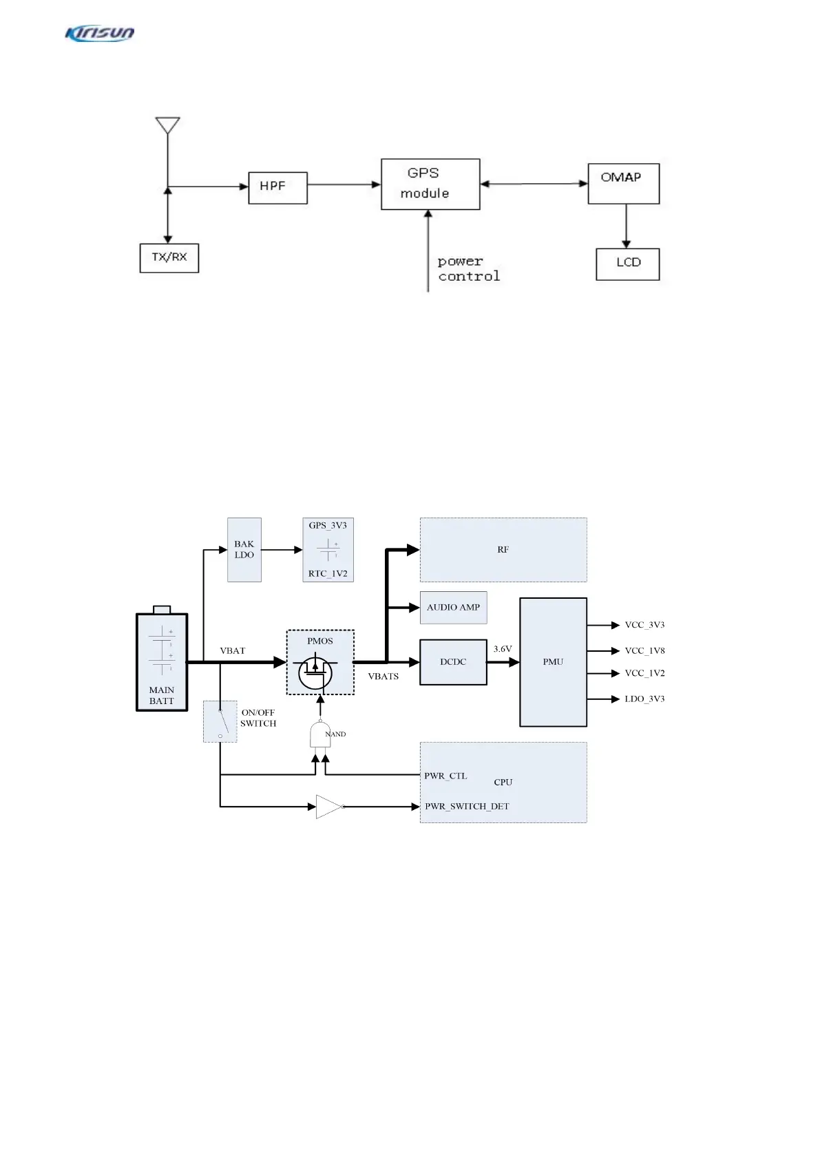
3.5.GPS Circuit
Positioning is achieved by the chip AT6558D-5N72. GPS/BDS signals are received by an antenna inductor, and
then pass an HPF to filter Tx/Rx in-band signals. The band and harmonic spurious signals are further suppressed.
Weak GPS/BDS signals pass a filter for frequency selection and then enter a GPS module for further amplification
and filtered. The signals are sent to a base band for positioning information calculation, which is then sent to an
OMAP DSP for processing. After processing, data is sent to the LCD screen for display.
3.6.Baseband Circuit
3.6.1. Power Supply Circuit
The baseband circuit is powered by two Lithium batteries MAI N BATT, with a voltage of 8.4V when fully charged
and a minimum protection voltage of 6.3V.
The MAIN BATT voltage passes a PMOS switch and undergoes two-stage conversion. The voltage is converted
into 3.6V through a DC-DC converter in the first stage, and four power supplies through a PMU in the second stage
to power every part of the baseband circuit.
The VBAT voltage provides through a BAK LDO a backup voltage to charge a button cell, which is used by the
GPS and RTC to maintain data and real-time clock. Another VBATS voltage is provided respectively to an analog
audio amplifier and an RF circuit.
During power-on, a power supply knob (ON/OFF SWITCH) is on, the PMOS grid is turned to a low level through a
set of control circuits, a MOS transistor is on, the whole device is powered on, the processor runs, the input port
PWR_SWITCH_DET detects a high-level power-on signal, and the output port PWR_CTL outputs a high level to
lock the low level at the PMOS grid to keep the MOS on.

 Loading...