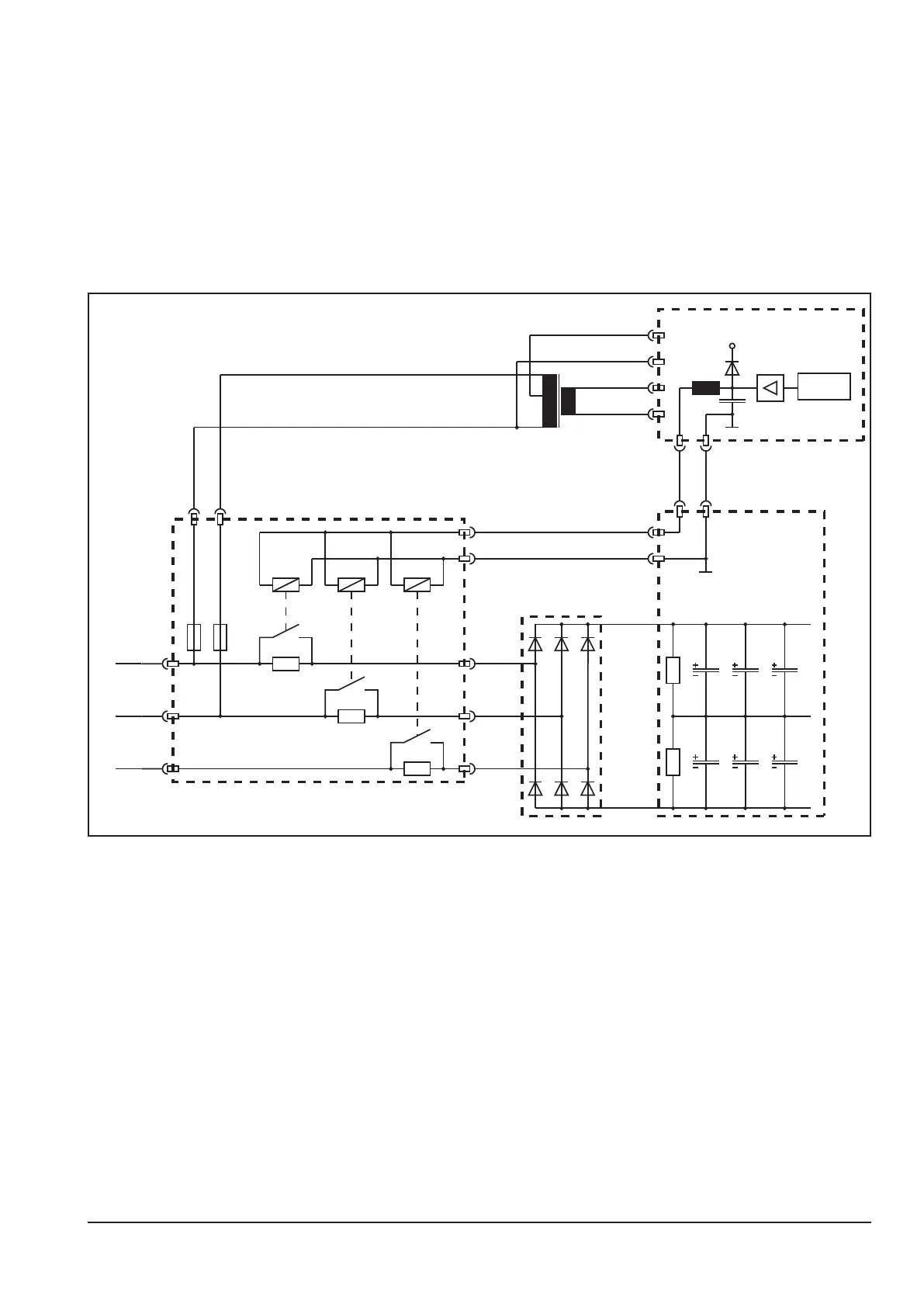
page 41
Power-up cycle
After switching on the machine with the mains switch, the capacitors on the DCDRV pcb are charged up rst.
These capacitors are buering the bus voltage (rectied mains voltage). The input current during charge up
can be very high and must be limited to prevent the mains fuses to break. The current limitation is made by the
PWRUP pcb, where each phase is conducted via resistors to the mains rectier. After the bus voltage reached
a certain voltage (>250V DC), the resistors on the PWRUP pcb are short circuit with relays, so the the full mains
input is present and the bus voltage is at maximum (560V DC to 580V DC).
The bus voltage is monitored by the DSP (Process) and the relays on the PWRUP board are switched by the
microcontroller (Master).
Schematic
X4 / 1
X4 / 2
X1
X2
X3
X5
X6
X7
L1
L2
L3
DK-PWRUP
X10 / 1
X10 / 2
X2 / 5
X2 / 6
X1 / 13
X1 / 7
DK-DCDRV
DK-MAPRO
+24V
Master
X9 / 1
X9 / 2
X6 / 1
X6 / 3