57
CS4392KZZ(AUDIO:IC75)
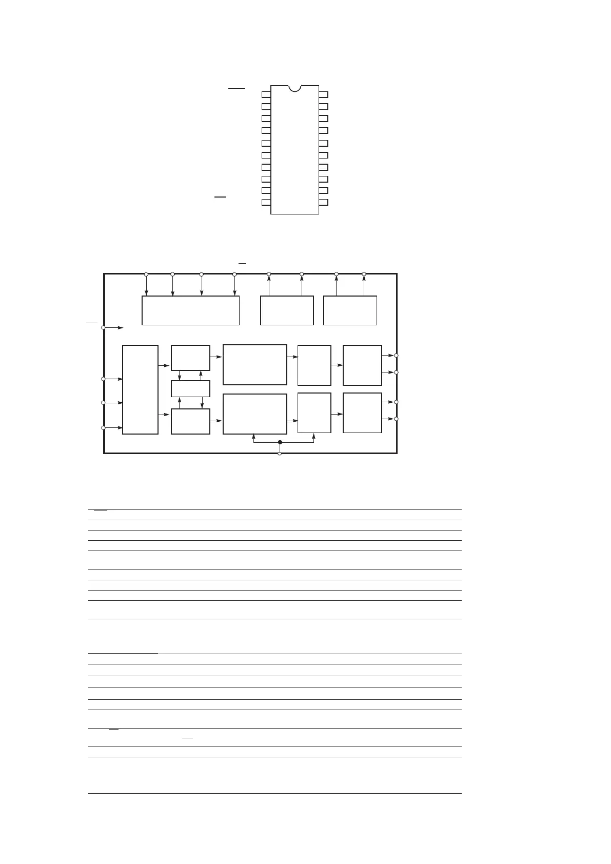
BlockDiagram
TerminalFunction
1. PIN DESCRIPTION - PCM DATA MODE
RST 1 Reset (Input) - Powers down device and resets all internal registers to their default settings.
VL 2 Logic Power (Input) - Positive power for the digital input/output.
SDATA 3 Serial Audio Data (Input) - Input for two’s complement serial audio data.
SCLK 4 Serial Clock (Input/Output) - Serial clock for the serial audio interface.
LRCK 5 Left Right Clock (Input/Output) - Determines which channel, Left or Right, is currently active on the
serial audio data line.
MCLK 6 Master Clock (Input) - Clock source for the delta-sigma modulator and digital filters.
FILT+ 11 Positive Voltage Reference (Output) - Positive reference voltage for the internal sampling circuits.
CMOUT 12 Common Mode Voltage (Output) - Filter connection for internal quiescent voltage.
AMUTEC
BMUTEC
20
13
Mute Control (Output) - The Mute Control pin goes high during power-up initialization, reset, muting,
power-down or if the master clock to left/right clock frequency ratio is incorrect.
AOUTB-
AOUTB+
AOUTA+
AOUTA
14
15
18
19
Differential Analog Output (Outputs) - The full scale differential analog output level is specified in the
Analog Characteristics specification table.
AGND 16 Ground (Input)
VA
17 Analog Power (Input) - Positive power for the analog section.
Control Port Mode Definitions
M3
7 Mode Selection (Input)
- This pins should be tied to GND level during control port mode.
SCL/CCLK 8 Serial Control Port Clock (Input) - Serial clock for the serial control port.
SDA/CDIN 9 Serial Control Data (Input/Output) - SDA is a data I/O line in I
2
C mode. CDIN is the input data line for
the control port interface in SPI mode.
AD0/CS 10 Address Bit 0 (I
2
C) / Control Port Chip Select (SPI) (Input/Output) - AD0 is a chip address pin in I
2
C
mode; CS is the chip select signal for SPI format.
Stand-Alone Mode Definitions
M3
M2
M1
M0
7
8
9
10
Mode Selection (Input) - Determines the operational mode of the device.
RST AMUTEC
VL AOUTA-
SDATA AOUTA+
SCLK VA
LRCK AGND
MCLK AOUTB+
M3 AOUTB-
(SCL/CCLK) M2 BMUTEC
(SDA/CDIN) M1 CMOUT
(AD0/CS
) M0 FILT+
1
2
3
4
20
19
18
17
5
6
7
8
16
15
14
13
9
10
12
11
Preliminary Product Information
This document contains information for a new product.
Cirrus Logic reserves the right to modify this product without notice.
Copyright © Cirrus Logic, Inc. 2002
(All Rights Reserved)
http://www.cirrus.com
CS4392
24-Bit, 192 kHz Stereo DAC with Volume Control
Features
z Complete Stereo DAC System: Interpolation,
D/A, Output Analog Filtering
z 114 dB Dynamic Range
z 100 dB THD+N
z Up to 192kHz Sample Rates
z Direct Stream Digital Mode
z Low Clock Jitter Sensitivity
z Single +5 V Power Supply
z Selectable Digital Filters
– Fast and Slow roll-off
z Volume Control with Soft Ramp
– 1 dB Step Size
– Zero Crossing Click-Free Transitions
z Direct Interface with 5 V to 1.8 V Logic
z ATAPI Mixing Functions
z Pin Compatible with the CS4391
Description
The CS4392 is a complete stereo digital-to-analog sys-
tem including digital interpolation, fifth-order delta-sigma
digital-to-analog conversion, digital de-emphasis, vol-
ume control, channel mixing and analog filtering. The
advantages of this architecture include: ideal differential
linearity, no distortion mechanisms due to resistor
matching errors, no linearity drift over time and tempera-
ture, and a high tolerance to clock jitter.
The CS4392 accepts PCM data at sample rates from
4 kHz to 192 kHz, DSD audio data, has selectable digital
filters, and consumes very little power. These features
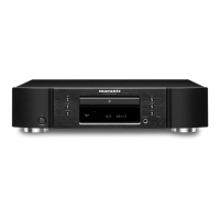
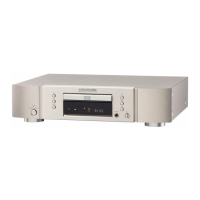
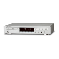
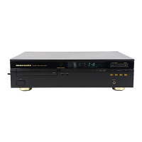
are ideal for DVD, SACD players, A/V receivers, CD and
set-top box systems. The CS4392 is pin and register
compatible with the CS4391, making easy performance
upgrades possible.
ORDERING INFORMATION
CS4392-KS -10 to 70 °C 20-pin SOIC
CS4392-KZ -10 to 70 °C 20-pin TSSOP
CS4392-KZZ, Lead Free -10 to 70 °C 20-pin TSSOP
CDB4392 Evaluation Board
I
LRCK
(SDA/CDIN)
MCLK
AMUTEC
AOUTA-
AOUTB-
SERIAL
PORT
INTERPOLATION
INTERPOLATION
(CONTROL PORT)
∆Σ
DAC
DAC
EXTERNAL
ANALOG
FILTER
ANALOG
FILTER
∆Σ
MUTE CONTROL
FILTER
FILTER
RST
SCLK
VOLUME
CONTROL
VOLUME
CONTROL
MIXER
(SCL/CCLK) (AD0/CS)
AOUTA+
AOUTB+
CMOUT
REFERENCE
FILT+BMUTEC
M1
M3
M2
MODE SELECT
M0
CS4392
DS459PP3 5
1. PIN DESCRIPTION - PCM DATA MODE
RST 1 Reset (Input) - Powers down device and resets all internal registers to their default settings.
VL 2 Logic Power (Input) - Positive power for the digital input/output.
SDATA 3 Serial Audio Data (Input) - Input for two’s complement serial audio data.
SCLK 4 Serial Clock (Input/Output) - Serial clock for the serial audio interface.
LRCK 5 Left Right Clock (Input/Output) - Determines which channel, Left or Right, is currently active on the
serial audio data line.
MCLK 6 Master Clock (Input) - Clock source for the delta-sigma modulator and digital filters.
FILT+ 11 Positive Voltage Reference (Output) - Positive reference voltage for the internal sampling circuits.
CMOUT 12 Common Mode Voltage (Output) - Filter connection for internal quiescent voltage.
AMUTEC
BMUTEC
20
13
Mute Control (Output) - The Mute Control pin goes high during power-up initialization, reset, muting,
power-down or if the master clock to left/right clock frequency ratio is incorrect.
AOUTB-
AOUTB+
AOUTA+
AOUTA
14
15
18
19
Differential Analog Output (Outputs) - The full scale differential analog output level is specified in the
Analog Characteristics specification table.
AGND 16 Ground (Input)
VA
17 Analog Power (Input) - Positive power for the analog section.
Control Port Mode Definitions
M3
7 Mode Selection (Input)
- This pins should be tied to GND level during control port mode.
SCL/CCLK 8 Serial Control Port Clock (Input) - Serial clock for the serial control port.
SDA/CDIN 9 Serial Control Data (Input/Output) - SDA is a data I/O line in I
2
C mode. CDIN is the input data line for
the control port interface in SPI mode.
AD0/CS
10 Address Bit 0 (I
2
C) / Control Port Chip Select (SPI) (Input/Output) - AD0 is a chip address pin in I
2
C
mode; CS
is the chip select signal for SPI format.
Stand-Alone Mode Definitions
M3
M2
M1
M0
7
8
9
10
Mode Selection (Input) - Determines the operational mode of the device.
RST AMUTEC
VL AOUTA-
SDATA AOUTA+
SCLK VA
LRCK AGND
MCLK AOUTB+
M3 AOUTB-
(SCL/CCLK) M2 BMUTEC
(SDA/CDIN) M1 CMOUT
(AD0/CS
) M0 FILT+
1
2
3
4
20
19
18
17
5
6
7
8
16
15
14
13
9
10
12
11