NCP380 (IC106)
NCP380 Terminal Function
Block Diagram
NCP380
http://onsemi.com
2
IN OUT
EN
ILIM*
GND
NCP380
USB
Port
GND
D+
D−
VBUS
Rlim
USB INPUT
5V
EN
FLAG
USB
DATA
Rfault
*
Figure 1. Typical Application Circuit
100 k
1 F
120 F
FLAG
*For adjustable version only.
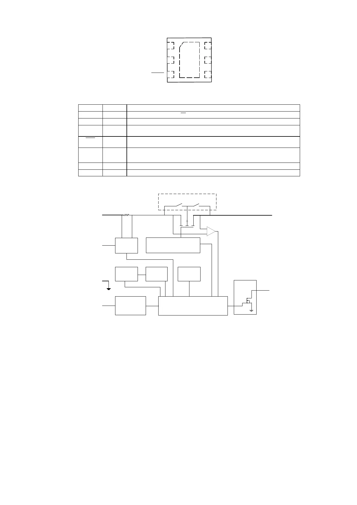
(Top view)
Figure 2. Pin Connections
1
2
3
6
5
4
OUT
ILIM*
FLAG
IN
GND
EN
PAD1
UDFN6
OUT
GND
FLAG
IN
EN
1
2
3
5
4
TSOP−5
1
2
3
6
4
OUT
ILIM*
5
FLAG
IN
GND
EN
TSOP−6
*For adjustable version only, otherwise not connected.
PIN FUNCTION DESCRIPTION
Pin Name Type Description
EN INPUT Enable input, logic low/high (i.e. EN or EN) turns on power switch
GND POWER Ground connection;
IN POWER
Power−switch input voltage; connect a 1 F or greater ceramic capacitor from IN to GND as close as
possible to the IC.
FLAG OUTPUT Active−low open−drain output, asserted during overcurrent, overtemperature or reverse−voltage
conditions. Connect a 10 k or greater resistor pull−up, otherwise leave unconnected.
OUT OUTPUT
Power−switch output; connect a 1 F ceramic capacitor from OUT to GND as close as possible to the IC
is recommended. A 1 F or greater ceramic capacitor from OUT to GND must be connected if the USB
requirement (i.e.120 F capacitor minimum) is not met.
ILIM* INPUT
External resistor used to set current−limit threshold; recommended 5 k < R
ILIM
< 250 k.
PAD1** THERMAL Exposed Thermal Pad: Must be soldered to PCB Ground plane
*(For adjustable version only, otherwise not connected.
**For DFN version only.
NCP380
http://onsemi.com
2
IN OUT
EN
ILIM*
GND
NCP380
USB
Port
GND
D+
D−
VBUS
Rlim
USB INPUT
5V
EN
FLAG
USB
DATA
Rfault
*
Figure 1. Typical Application Circuit
100 k
1 F
120 F
FLAG
*For adjustable version only.
(Top view)
Figure 2. Pin Connections
1
2
3
6
5
4
OUT
ILIM*
FLAG
IN
GND
EN
PAD1
UDFN6
OUT
GND
FLAG
IN
EN
1
2
3
5
4
TSOP−5
1
2
3
6
4
OUT
ILIM*
5
FLAG
IN
GND
EN
TSOP−6
*For adjustable version only, otherwise not connected.
PIN FUNCTION DESCRIPTION
Pin Name Type Description
EN INPUT Enable input, logic low/high (i.e. EN or EN) turns on power switch
GND POWER Ground connection;
IN POWER
Power−switch input voltage; connect a 1 F or greater ceramic capacitor from IN to GND as close as
possible to the IC.
FLAG OUTPUT Active−low open−drain output, asserted during overcurrent, overtemperature or reverse−voltage
conditions. Connect a 10 k or greater resistor pull−up, otherwise leave unconnected.
OUT OUTPUT
Power−switch output; connect a 1 F ceramic capacitor from OUT to GND as close as possible to the IC
is recommended. A 1 F or greater ceramic capacitor from OUT to GND must be connected if the USB
requirement (i.e.120 F capacitor minimum) is not met.
ILIM* INPUT
External resistor used to set current−limit threshold; recommended 5 k < R
ILIM
< 250 k.
PAD1** THERMAL Exposed Thermal Pad: Must be soldered to PCB Ground plane
*(For adjustable version only, otherwise not connected.
NCP380
http://onsemi.com
7
BLOCK DIAGRAM
Gate Driver
UVLO
Vref
TSD
Control logic
and timer
EN block
Flag
Osc
IN
OUT
/FLAG
GND
EN
Blocking control
Current
Limiter
ILIM*
Figure 5. Block Diagram
*For adjustable version only, otherwise not connected.
NCP380
PMOSFET
MOSFET
¡
¢£¤¥¦§¨©ª«¬
®¯°±NCP380²³
´µ¶´·¸¦±
NCP380¹°I
OCP
§
¯º»º¼½¾¿ÀÁ¿¹
ÂÃÄ¥
− ÅÆǨ«ª¹
ÈÉÄ¥NCP380
ÈÉÊ°ËÌI
OCP
§
ͦ¥
VOUT
IOCP
IOUT
Drop due to
capacitor charge
Figure 6. Heavy capacitive load
− ÎI
OCP
ͦÍ
ÂÃÏÐѵĥ
V
OUT
R
LOAD
I
OCP
(eq. 1)
65