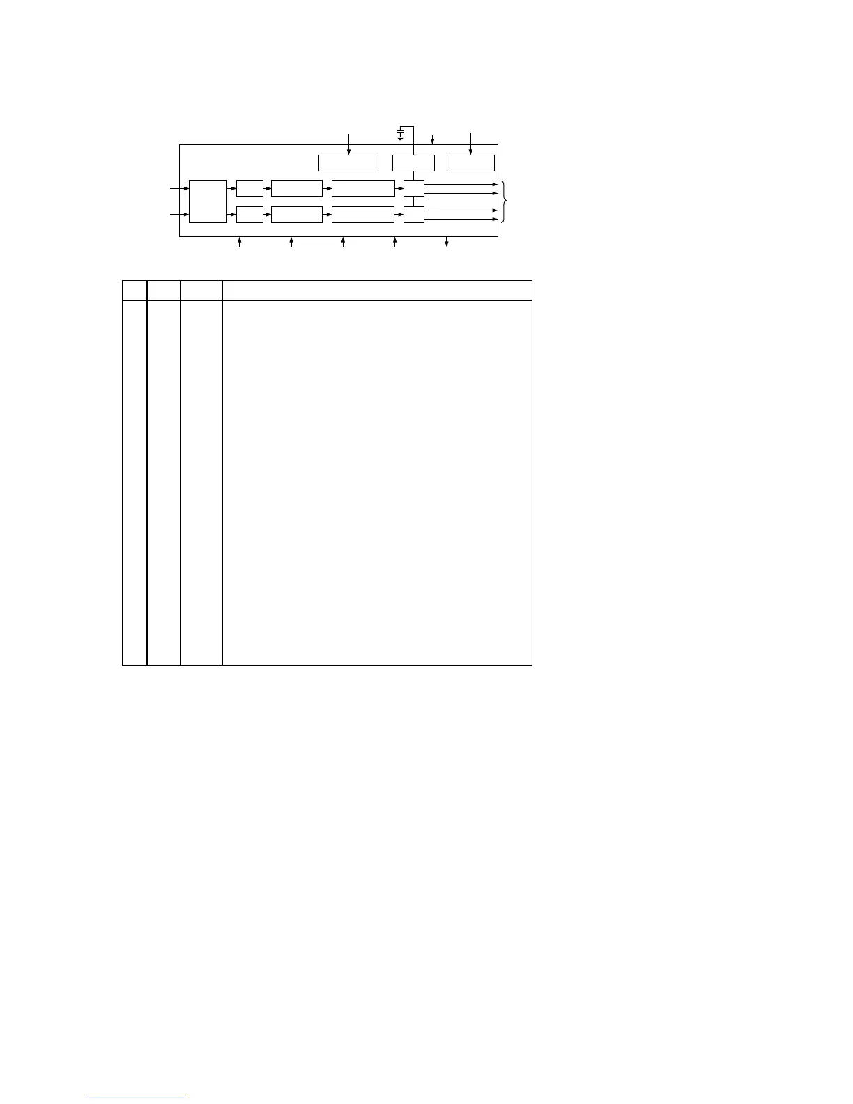
41
SERIAL
DATA
INTERFACE
8 x Fs
INTERPOLATOR
SERIAL CONTROL
INTERFACE
AUTO-CLOCK
DIVIDE CIRCUIT
VOLUME
MUTE
CONTROL DATA
INPUT
3
2
DIGITAL
SUPPLY
CLOCK
IN
ANALOG
OUTPUTS
22
ZERO
FLAG
ANALOG
SUPPLY
DE-EMPHASISMUTE
RESET
2
SERIAL
MODE
16-/18-/20-/24-BIT
DIGITAL
DATA INPUT
AD1852
MULTIBIT SIGMA-
DELTA MODULATOR
ATTEN/
MUTE
DAC
MULTIBIT SIGMA-
DELTA MODULATOR
8 x Fs
INTERPOLATION
ATTEN/
MUTE
VOLTAGE
REFERENCE
DAC
I
Pin
Input/
Output
Pin Name Description
1 DGND Digital Ground.
2MCLK
Master Clock Input. Connect to an external clock source at either 256 FS, 384 FS, 512 FS,
768 FS, or 1024 FS.
3
I
I
I CLATCH Latch Input for Control Data. This input is rising-edge sensitive.
4 CCLK
Control Clock Input for Control Data. Control input data must be valid on the rising edge of
CCLK. CCLK may be continuous or gated.
5 CDATA
Serial Control Input, MSB first, containing 16 bits of unsigned data per channel. Used for
specifying channel-specific attenuation and mute.
6 NC No Connect.
7 I 192/48 Selects 48 kHz (LO) or 192 kHz Sample Frequency.
8 ZEROR
Right Channel Zero Flag Output. This pin goes HI when Right Channel has no signal
input for more than 1024 LR Clock Cycles.
9 DEEMP
De-Emphasis. Digital de-emphasis is enabled when this input signal is HI. This is used to
impose a 50 µs/15 µs response characteristic on the output audio spectrum at an assumed
44.1 kHz sample rate. Curves for 32 kHz and 48 kHz sample rates may be selected via SPI
control register.
10 I 96/48 Selects 48 kHz (LO) or 96 kHz Sample Frequency.
11, 15 I AGND Analog Ground.
12 O OUTR+ Right Channel Positive Line Level Analog Output.
13 O OUTR– Right Channel Negative Line Level Analog Output.
14 O FI LTR
Voltage Reference Filter Capacitor Connection. Bypass and decouple the voltage reference
with parallel 10 µF and 0.1 µF capacitors to the AGND.
16 O OUTL– Left Channel Negative Line Level Analog Output.
17 O OUTL+ Left Channel Positive Line Level Analog Output.
18 I AVDD Analog Power Supply. Connect to Analog 5 V Supply.
19 FILTB Filter Capacitor Connection. Connect 10 µF capacitor to AGND (Pin 15).
20 I IDPM1 Input Serial Data Port Mode Control One. With IDPM0, defines 1 of 4 serial modes.
21 I IDPM0 Input Serial Data Port Mode Control Zero. With IDPM1, defines 1 of 4 serial modes.
22 O ZE ROL
Left Channel Zero Flag Output. This pin goes HI when Left Channel has no signal input for
more than 1024 LR Clock Cycles.
23 I MUTE Mute. Assert HI to mute both stereo analog outputs. Deassert LO for normal operation.
24 I R ESET
Reset. The AD1852 is reset on the rising edge of this signal. The serial control port registers
are reset to the default values. Connect HI for normal operation.
25 I L/RCLK Left/Right Clock Input for Input Data. Must run continuously.
26 I B CLK
Bit Clock Input for Input Data. Need not run continuously; may be gated or used in a burst
fashion.
27 I SD ATA
Serial Input, MSB first, containing two channels of 16, 18, 20, and 24 bits of twos complement
data per channel.
28 I DVDD Digital Power Supply Connect to digital 5 V supply.
TableI. Serial Data Input Mode
IDPM1 (Pin 20) IDPM0 (Pin 21) Serial Data Input Format
0 0 Right-Justified
0 1 I
2
S-Compatible
1 0 Left-Justified
1 1 DSP
I
I
O
QD02 - QD04 : AD1852