43
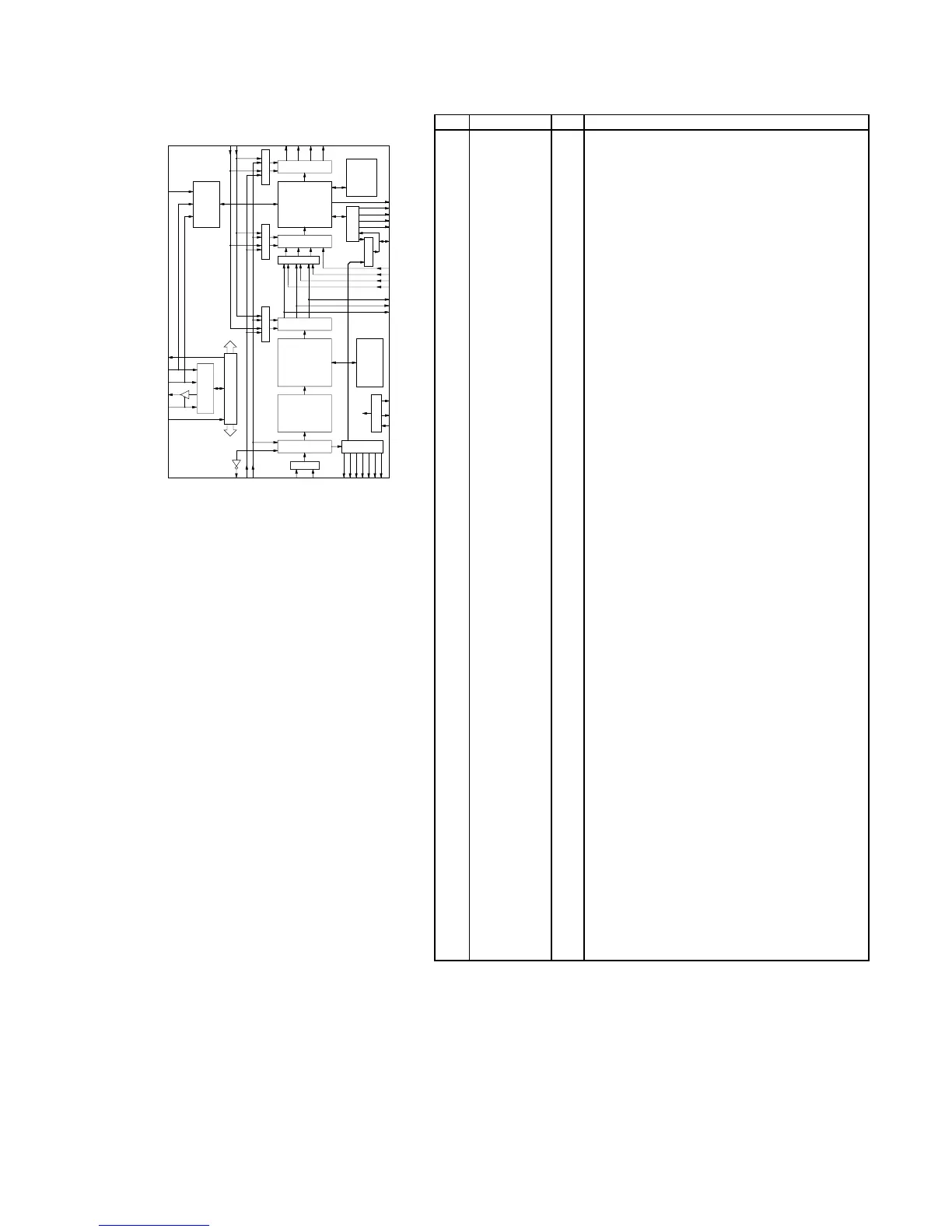
No. Name I/O FUNCTION
1 VDD1 - +5V power suppl
2 RAMCEN O External SRAM interface /CE
3 RAMA16 O External SRAM interface address 16
4 RAMA15 O External SRAM interface address 15
5 SDIB0 I+ PCM input 0 to Sub DSP
6 SDIB1 I+ PCM input 1 to Sub DSP
7 SDIB2 I+ PCM input 2 to Sub DSP
8XIICr
stal oscillator connection
stal oscillator connection
10 VSS - Ground
11 AVDD - +3.3 V power suppl
12 SDIB3 I+ PCM input 3 to Sub DSP
13 TEST Test terminal
15 OVFB O Detection of overflow at Sub DSP
16 DTSDATA O Detection of DTS data
17 AC3DATA O Detection of AC-3 data
18 SDOB3 O PCM output from Sub DSP
19 CPO A Output terminal for PLL, to be connected to ground
throu
filter circuit
20 AVSS - Ground
21 VDD2 - +3.3 V power suppl
22 SDOA2 O PCM output from Main DSP
23 SDOA1 O PCM output from Main DSP
24 SDOA0 O PCM output from Main DSP
25 RAMA14 O External SRAM interface address 14
26 RAMA13 O External SRAM interface address 13
27 RAMA12 O External SRAM interface address 12
28 RAMA11 O External SRAM interface address 11
29 RAMA10 O External SRAM interface address 10
30 VSS - Ground
31 VDD1 - +5V power suppl
32 OPORT0 O Output port for
eneral purpose
33 OPORT1 O Output port for
eneral purpose
34 OPORT2 O Output port for
eneral purpose
35 OPORT3 O Output port for
eneral purpose
36 OPORT4 O Output port for
eneral purpose
37 OPORT5 O Output port for
eneral purpose
38 OPORT6 O Output port for
eneral purpose
39 OPORT7 O Output port for
eneral purpose
40 VSS - Ground
41 VDD2 - +3.3 V power suppl
42 RAMA9 O External SRAM interface address 9
43 RAMA8 O External SRAM interface address 8
44 RAMA7 O External SRAM interface address 7
45 SDOB2 O PCM output from Sub DSP
46 SDOB1 O PCM output from Sub DSP
47 SDOB0 O PCM output from Sub DSP
48 SDBCK1 I+ Bit clock input for SDOA, SDIB, SDOB
49 SDWCK1 I+ Word clock input for SDOA, SDIB, SDOB
50 VSS - Ground
51 VDD2 - +3.3 V power suppl
52 NONPCM O Detection of non-PCM data
53 CRC O Detection of AC-3 CRC error
54 MUTE O Detection of auto mute
55 KARAOKE O Detection of AC-3 karaoke data
CPO
XO
XI
SDOB0
SDOB1
SDOB2
SDWCK1
SDBCK1
OPORT0-7
IPORT0-7
SO
SI
SCK
/CS
OVFB
RAMA0-16
RAMOEN
RAMWEN
RAMCEN
RAMD0-7
SDIB2
SDIB1
SDIB0
SDOA2
SDOA1
SDOA0
Delay RAM
SDIASEL
SDIA1
SDIA0
SDWCK0
SDBCK0
/SDBCK0
/CSB
SCK
SI
SDOACKSEL SDIBCKSEL
SDOBCKSEL
Operating clock
(30MHz)
CRC
ERAMUSE
External RAM
SDOB Interface
24 * 16
Sub DSP
SDIB Interface
SDOA Interface
SDIBSEL
SDIA Interface
Input Buffer
decoder
24 * 24
Main DSP
AC-3/Pro Logic/DTS
Data RAM
Microprocessor
Control Registers
Control signals
Coefficient /
Program RAM
STREAM0-7
PLL
L, R
LS, RS
C, LFE
SDOB3
SDIB3
SURENC
KARAOKE
MUTE
CRC
AC3DATA
DTSDATA
NONPCM
Interface
Control signals
interface
Q601 : YSS912