167
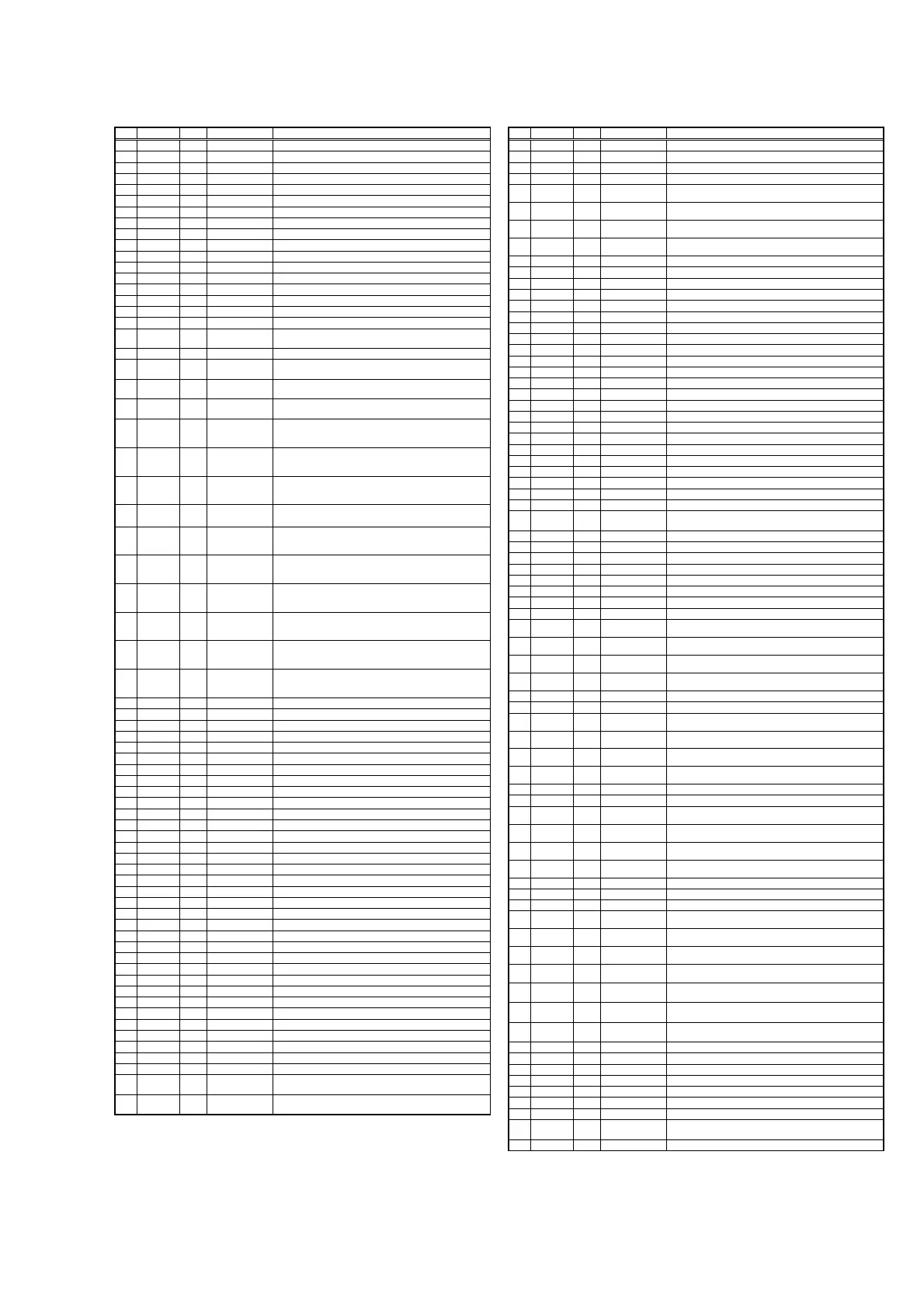
IC63 : CD0040AF
No. Name I/O
1
Attr ibut e Functional Description
70 OVSS P - Digital ground for Pad Ring
71 CVDD P - Digital positive supply voltage (+2.5V) for core
72 IVDD P - Positive supply voltage (+3.3V) for Pad Ring
73 OVDD P - Positive supply voltage (+3.3V) for Pad Ring
74 MD19 Inout
CMOS, pull-up /
4mA
Data input/output port for SDRAM
75 MD18 Inout
CMOS, pull-up /
4mA
Data input/output port for SDRAM
76 MD17 Inout
CMOS, pull-up /
4mA
Data input/output port for SDRAM
77 MD16 Inout
CMOS, pull-up /
4mA
Data input/output port for SDRAM
78 OVDD P - Positive supply voltage (+3.3V) for Pad Ring
79 OVSS P - Digital ground for Pad Ring
80 MA3 Out 4mA Address output port for SDRAM
81 MA4 Out 4mA Address output port for SDRAM
82 MA2 Out 4mA Address output port for SDRAM
83 MA5 Out 4mA Address output port for SDRAM
84 OVDD P - Positive supply voltage (+3.3V) for Pad Ring
85 OVSS P - Digital ground for Pad Ring
86 MA1 Out 4mA Address output port for SDRAM
87 MA6 Out 4mA Address output port for SDRAM
88 MA0 Out 4mA Address output port for SDRAM (LSB)
89 MA7 Out 4mA Address output port for SDRAM
90 OVSS P - Digital ground for Pad Ring
91 IVSS P - Digital ground for Pad Ring
92 CVSS P - Digital ground for Pad Ring for Core
93 OVDD P - Positive supply voltage (+3.3V) for Pad Ring
94 MA10 Out 4mA Address output port for SDRAM
95 MA8 Out 4mA Address output port for SDRAM
96 MA11 Out 4mA Address output port for SDRAM (MSB)
97 MA9 Out 4mA Address output port for SDRAM
98 OVDD P - Positive supply voltage (+3.3V) for Pad Ring
99 OVSS P - Digital ground for Pad Ring
100 RAS Out 4mA Row Address Strobe command output port for SDRAM
101 DQM Out 4mA
DQM output port for SDRAM. In addition, please connect the
CKE terminal of SDRAM to the power supply of SDRAM
102 CAS Out 4mA Column Address Strobe command o utput port for SDRAM
103 MCLK Out 4mA Clock output port for SDRAM (54MHz)
104 WE Out 4mA Write Enable output port for SDRAM
105 TEST3 In CMOS Test purpose only (must be connected to ground)
106 TEST4 In CMOS Test purpose only (must be connected to ground)
107 OVSS P - Digital ground for Pad Ring
108 OVDD P - Positive supply voltage (+3.3V) for Pad Ring
109 CVDD P - Digital positive supply voltage (+2.5V) for core
110 MD7 Inout
CMOS, pull-up /
4mA
Data input/output port for SDRAM
111 MD8 Inout
CMOS, pull-up /
4mA
Data input/output port for SDRAM
112 MD6 Inout
CMOS, pull-up /
4mA
Data input/output port for SDRAM
113 MD9 Inout
CMOS, pull-up /
4mA
Data input/output port for SDRAM
114 OVDD P - Positive supply voltage (+3.3V) for Pad Ring
115 OVSS P - Digital ground for Pad Ring
116 MD5 Inout
CMOS, pull-up /
4mA
Data input/output port for SDRAM
117 MD10 Inout
CMOS, pull-up /
4mA
Data input/output port for SDRAM
118 MD4 Inout
CMOS, pull-up /
4mA
Data input/output port for SDRAM
119 MD11 Inout
CMOS, pull-up /
4mA
Data input/output port for SDRAM
120 OVDD P
-
Positive supply voltage (+3.3V) for Pad Ring
121 OVSS P
-
Digital ground for Pad Ring
122 MD3 Inout
CMOS, pull-up /
4mA
Data input/output port for SDRAM
123 MD12 Inout
CMOS, pull-up /
4mA
Data input/output port for SDRAM
124 MD2 Inout
CMOS, pull-up /
4mA
Data input/output port for SDRAM
125 MD13 Inout
CMOS, pull-up /
4mA
Data input/output port for SDRAM
126 OVSS P
-
Digital ground for Pad Ring
127 CVSS P
-
Digital ground for core
128 OVDD P
-
Positive supply voltage (+3.3V) for Pad Ring
129 MD1 Inout
CMOS, pull-up /
4mA
Data input/output port for SDRAM
130 MD14 Inout
CMOS, pull-up /
4mA
Data input/output port for SDRAM
131 MD0 Inout
CMOS, pull-up /
4mA
Data input/output port for SDRAM
132 MD15 Inout
CMOS, pull-up /
4mA
Data input/output port for SDRAM
133 SLV In CMOS
Slave address selection input for I2C. Slave address is set up
to 0x72 when SLV is “0”, 0x70 when “1”.
134 RFFO Out 2mA
MPEG flag (Repeat First Field) output port. If not used, leave
open.
135 SDA Inout
Schmitt, 3.3V /
4mA
Data input/output of MPU interface
136 SCL In Schmitt, 3.3V Clock input of MPU interface
137 SRN In Schmitt System reset input(negative)
138 OVSS P - Digital ground for Pad Ring
139 CVDD P - Digital positive supply voltage (+2.5V) for core
140 PLL_VDD P - Digital positive supply voltage (+2.5V) for PLL
141 VPDX In CMOS Must be connected to ground
142 TEST6 In CMOS Test purpose only (must be connected to ground)
143
PLL_GN
D
P - Ground for PLL
144 IVDD P - Positive supply voltage (+3.3V) for Pad Ring
Note: *1 P10 and P11 should be connected to GND at the time of 8bit input.
*2 PO0 and PO1 should connected to GND at the time of 8bit input.
*3 Although the same bidirectional buffer as PO is used in order to unite PO and timing at the time of PO
input, it is always fixed as an input.
*4 The initial-setting value or the initial state in a reset period and after reset release.
No. Name I/O
1
Attr ibut e Functional Description
1 OVDD P - Positive supply voltage(+3.3V) for Pad Ring
2 CLKI In CMOS System Clock Input (27MHz)
3 TEST7 In CMOS Test purpose only(must be connected to Ground)
4 PLL_EN In CMOS PLL enable
5 PI0 In CMOS ITU-R BT.656/601 Input (LSB)
6 PI1 In CMOS ITU-R BT.656/601 Input
7 PI2 In CMOS ITU-R BT.656/601 Input
8 PI3 In CMOS ITU-R BT.656/601 Input
9 PI4 In CMOS ITU-R BT.656/601 Input
10 PI5 In CMOS ITU-R BT.656/601 Input
11 PI6 In CMOS ITU-R BT.656/601 Input
12 PI7 In CMOS ITU-R BT.656/601 Input
13 PI8 In CMOS ITU-R BT.656/601 Input
14 PI9 In CMOS ITU-R BT.656/601 Input (MSB)
15 NHSI In Schmitt Active low horizontal sync input
16 NVSI In Schmitt Active low vertical sync input
17 OVSS P - Digital ground for Pad Ring
18 THMD In Schmitt
Through mode setting terminal. Usually, this must be
connected to ground.
19 CVSS P - Digital ground for Core
20 NVSO Out 2mA
Active low vertical sync output (Interlace or Progressive)
Refer “11.2Video Output”
21 NHSO Out 2mA
Active low horizontal sync output(Interlace or Progressive)
Refer “11.2Video Output”
22 PO9 Inout CMOS / 2mA
ITU-R BT.656/601 output (MSB) / clamp signal output / ITU-R
BT. 601 Cb Cr input(MSB)
23 PO8 Inout CMOS / 2mA
ITU-R BT.656/601 output / Video active signal output / ITU-R
BT. 601 CbCr input. Refer “11.1Video Input””11.2Video
Output””11.3Through Mode”
24 PO7 Inout CMOS / 2mA
ITU-R BT.656/601 output / Video blanking signal output /
ITU-R BT. 601 CbCr input
Refer “11.1Video Input””11.2Video Output”
25 PO6 Inout CMOS / 2mA
ITU-R BT.656/601 output / ITU-R BT.601 CbCr input
Refer “11.1Video Input””11.2Video Output”11.3Through
Mode”
26 OVDD P - Positive supply voltage (+3.3V) for Pad Ring
27 OVSS P - Digital ground for Pad Ring
28 PO5 Inout CMOS / 2mA
ITU-R BT.656/601 output / ITU-R BT.601 CbCr input
Refer “11.1Video Input””11.2Video Output””11.3Through
Mode”
29 PO4 Inout CMOS / 2mA
ITU-R BT.656/601 output / ITU-R BT.601 CbCr input
Refer “11.1Video Input””11.2Video Output””11.3Through
Mode”
30 PO3 Inout CMOS / 2mA
ITU-R BT.656/601 output / ITU-R BT.601 CbCr input
Refer “11.1Video Input””11.2Video Output””11.3Through
Mode”
31 PO2 Inout CMOS / 2mA
ITU-R BT.656/601 output / ITU-R BT.601 CbCr input
Refer “11.1Video Input””11.2Video Output””11.3Through
Mode”
32 PO1 Inout CMOS / 2mA
ITU-R BT.656/601 output / ITU-R BT.601 CbCr input
*2
Refer “11.1Video Input””11.2Video Output””11.3Through
Mode”
33 PO0 Inout CMOS / 2mA
ITU-R BT.656/601 output (LSB) / ITU-R BT.601 CbCr input
*2
Refer “11.1Video Input””11.2Video Output””11.3Through
Mode”
34 TEST0 In CMOS Test purpose only (must be connected to ground)
35 OVSS P - Digital ground for Pad Ring
36 OVDD P - Positive supply voltage (+3.3V) for Pad Ring
37 CVDD P - Digital positive supply voltage (+2.5V) for core
38 TEST1 In CMOS Test purpose only (must be connected to ground)
39 TEST2 In CMOS Test purpose only (must be connected to ground)
40 CLKO Out 2mA Clock output(27MHz)
41 YO9 Out 4mA ANSI/SMPTE 293M Y output(MSB)
42 YO8 Out 4mA ANSI/SMPTE 293M Y output
43 YO7 Out 4mA ANSI/SMPTE 293M Y output
44 YO6 Out 4mA ANSI/SMPTE 293M Y output
45 YO5 Out 4mA ANSI/SMPTE 293M Y output
46 OVDD P - Positive supply voltage (+3.3V) for Pad Ring
47 OVSS P - Digital ground for Pad Ring
48 YO4 Out 4mA ANSI/SMPTE 293M Y output
49 YO3 Out 4mA ANSI/SMPTE 293M Y output
50 YO2 Out 4mA ANSI/SMPTE 293M Y output
51 YO1 Out 4mA ANSI/SMPTE 293M Y output
52 YO0 Out 4mA ANSI/SMPTE 293M Y output (LSB)
53 OVDD P - Positive supply voltage (+3.3V) for Pad Ring
54 CVSS P - Digital ground for core
55 OVSS P - Digital ground for Pad Ring
56 CO0 Out 4mA ANSI/SMPTE 293M Cb/Cr output
57 CO1 Out 4mA ANSI/SMPTE 293M Cb/Cr output
58 CO2 Out 4mA ANSI/SMPTE 293M Cb/Cr output
59 CO3 Out 4mA ANSI/SMPTE 293M Cb/Cr output
60 CO4 Out 4mA ANSI/SMPTE 293M Cb/Cr output
61 OVDD P - Positive supply voltage (+3.3V) for Pad Ring
62 OVSS P - Digital ground for Pad Ring
63 CO5 Out 4mA ANSI/SMPTE 293M Cb/Cr output
64 CO6 Out 4mA ANSI/SMPTE 293M Cb/Cr output
65 CO7 Out 4mA ANSI/SMPTE 293M Cb/Cr output
66 CO8 Out 4mA ANSI/SMPTE 293M Cb/Cr output
67 CO9 Out 4mA ANSI/SMPTE 293M Cb/Cr output (MSB)
68 FILM Out 2mA
Film sequence detection flag output. Refer ”11.4.1.9Film
detection Flag Output”
69 RFFI In CMOS
MPEG flag (Repeat First Field) input port. Refer”11.4.1.6Film
I/P Conversion””11.4.1.8Film Sequence Flag Control Mode”
 Loading...