168
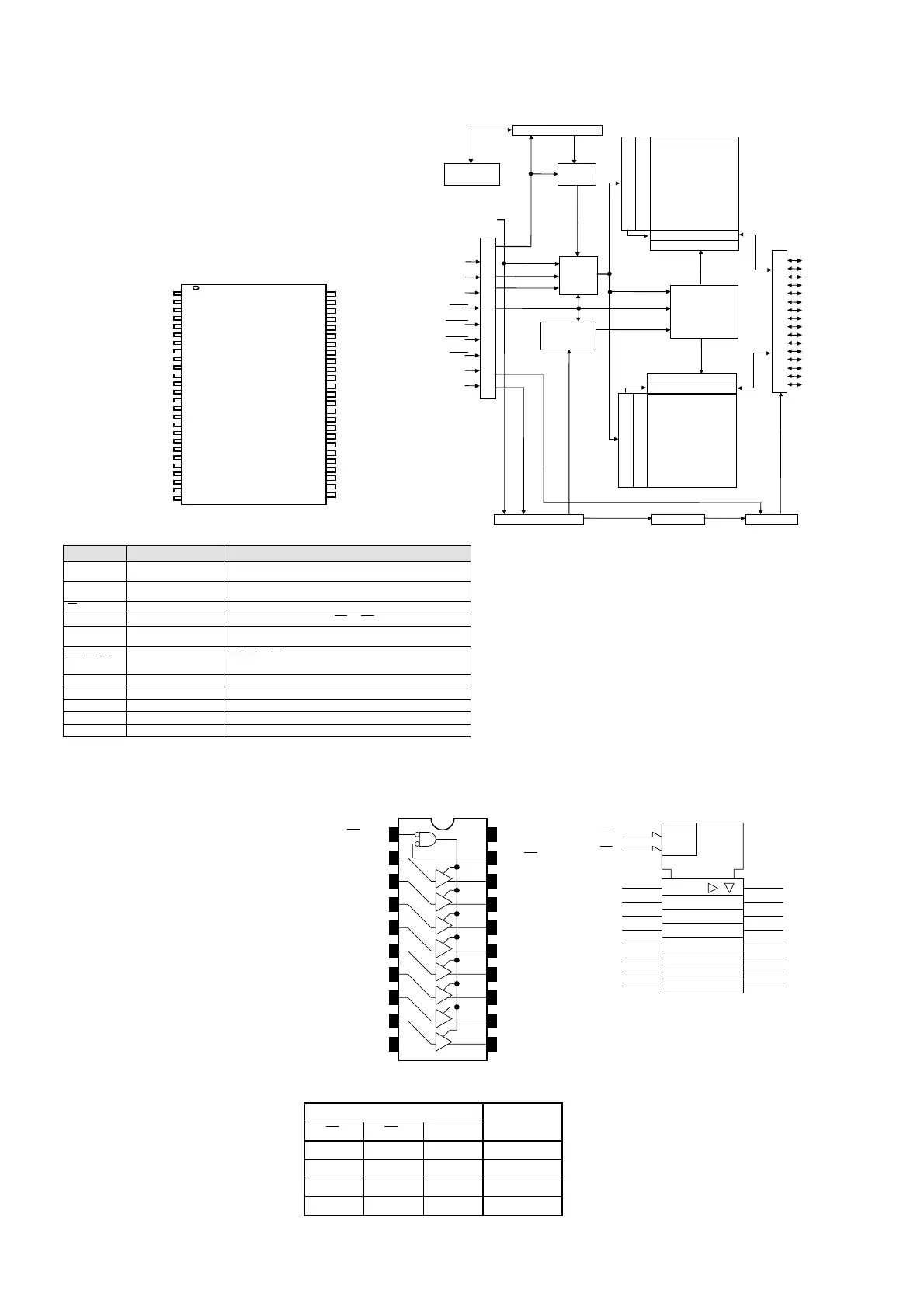
IC64 : HY57V161610ET-7
PIN CONFIGURATION
V
SS
DQ15
DQ14
VSSQ
DQ13
DQ12
VDDQ
DQ11
DQ10
VSSQ
DQ9
DQ8
VDDQ
NC
UDQM
CLK
CKE
NC
A9
A8
A7
A6
A5
A4
VSS
1
2
3
4
5
6
7
8
9
10
11
12
13
14
15
16
17
18
19
20
21
22
23
24
25
50
49
48
47
46
45
44
43
42
41
40
39
38
37
36
35
34
33
32
31
30
29
28
V
DD
DQ0
DQ1
V
SSQ
DQ2
DQ3
V
DDQ
DQ4
DQ5
V
SSQ
DQ6
VDDQ
/WE
/CAS
/RAS
/CS
A11
A10
A0
A1
A2
A3
V
DD
50pin TSOP II
400mil x 825mil
0.8mm pin pitch
27
26
DQ7
LDQM
V
SS
DQ15
DQ14
VSSQ
DQ13
DQ12
VDDQ
DQ11
DQ10
VSSQ
DQ9
DQ8
VDDQ
NC
UDQM
CLK
CKE
NC
A9
A8
A7
A6
A5
A4
VSS
1
2
3
4
5
6
7
8
9
10
11
12
13
14
15
16
17
18
19
20
21
22
23
24
25
50
49
48
47
46
45
44
43
42
41
40
39
38
37
36
35
34
33
32
31
30
29
28
V
DD
DQ0
DQ1
V
SSQ
DQ2
DQ3
V
DDQ
DQ4
DQ5
V
SSQ
DQ6
VDDQ
/WE
/CAS
/RAS
/CS
A11
A10
A0
A1
A2
A3
V
DD
50pin TSOP II
400mil x 825mil
0.8mm pin pitch
27
26
DQ7
LDQM
PIN DESCRIPTION
PIN PIN NAME DESCRIPTION
CLK Clock
The system clock input. All other inputs are referenced to the SDRAM on the rising
edge of CLK.
CKE Clock Enable
Controls internal clock signal and when deactivated, the SDRAM will be one of the
states among power down, suspend or self refresh.
CS
Chip Select Command input enable or mask except CLK, CKE and DQM
BA Bank Address Select either one of banks during both RAS and CAS activity.
A0 ~ A10 Address
Row Address : RA0 ~ RA10, Column Address : CA0 ~ CA7
Auto-precharge flag : A10
RAS, CAS, WE
Row Address Strobe,
Column Address Strobe, Write
Enable
RAS, CAS and WE define the operation.
Refer function truth table for details
LDQM, UDQM Data Input/Output Mask DQM control output buffer in read mode and mask input data in write mode
DQ0 ~ DQ15 Data Input/Output Multiplexed data input / output pin
V
DD/VSS Power Supply/Ground Power supply for internal circuit and input buffer
VDDQ/VSSQ Data Output Power/Ground Power supply for DQ
NC No Connection No connection
1Mx16 Synchronous DRAM
Column Addr.
Latch & Counter
Burst Length
Counter
Refresh
Interval Timer
Refresh
Counter
DQ0
DQ1
DQ2
DQ3
DQ4
DQ5
DQ6
DQ7
DQ8
DQ9
DQ10
DQ11
DQ12
DQ13
DQ14
DQ15
Address
Register
I/O ControlTest ModeMode Register
Self Refresh Counter
Column Decoder
Sense AMP & I/O gates
512Kx16
Bank 0
Column Decoder
Sense AMP & I/O gates
512Kx16
Bank 1
RAS
CAS
CS
WE
UDQM
LDQM
CKE
Precharge
Overflow
Column Active
Row Active
Address[0:10]
CLK
BA(A11)
State Machine
Row Decoder
Row Addr. Latch/Predecoder
Auto/Self Refresh
Ref. Addr.[0:11]
Data Input/Output Buffers
Row Addr. Latch/Predecoder
IC65 : TC74VCX541FT
IC66 : TC74VCX541FT
IC67 : TC74VCX541FT
IC68 : TC74VCX541FT
IC69 : TC74VCX541FT
IC70 : TC74VCX541FT
Pin Assignment
(top view)
IEC Logic Symbol
Truth Table
Inputs
1OE 2OE An
Outputs
H X X Z
X H X Z
L L H H
L L L L
X: Don’t care
Z: High impedance
V
CC
20
2OE
Y1
Y2
Y3
Y4
19
18
17
16
15
14
1OE 1
2
3
4
5
6
7
A1
A2
A3
A4
A5
A6 Y5
8
9
10
A7
A8
GND
13
12
11
Y6
Y7
Y8
2OE
(19)
(1)
(2)
(4)
(3)
A8
A2
A1
(6)
(5)
(8)
(7)
(9)
A3
A6
A5
A7
(18)
(16)
(14)
(12)
Y8
Y2
Y4
Y6
(17)
(15)
(13)
Y1
Y3
Y5
EN
(11)
Y7
A4
1OE
&