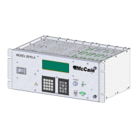
2070LX Controller – User Manual 15
Version 1.0
The 3.0VDC/5VDC dual supervisory power control switches supply 500mA minimum and limit fault
currents to 2A, the flag output pin for each switch is available to indicate fault conditions to the USB
controller. The soft start feature eliminates a momentary voltage drop on the upstream port that may
occur when the switch is enabled in bus-powered applications. The thermal shutdown feature prevents
damage to the device when subjected to excessive current loads. The under voltage lockout feature
ensures that the device remain off unless there is a valid input voltage present. There are three dual
supervisory power control switches on the Host Board, one for supplying power to the USB host controller
and one for supplying power to each port on the USB receptacles.
Common mode chokes are suited for common mode noise suppression on the USB lines because of the
large current flow. The USB host port from the Engine Board enters to the hub controller through common
mode chokes and also the downstream ports enter to the USB receptacles and connection headers
through common mode chokes.
2.4.1.9 Datakey circuitry
This circuit consists of a serial memory key receptacle which contains a Last-On/First-OF (LOFO) switch
that ensures the key does a secure contact before any signal is transmitted and support circuitry for
interfacing it with the processor.
It is implemented by using a DATAKEY receptacle KC4210PCB, three buffer gates and one PNP
transistor.
For any Data Key operation the data key driver samples the LOFO line, if the line is cleared (logic low
0VDC) the driver powers up the data key to begin the requested operation. After the operation is finished
the data key is powered down until another operation is requested.
Once the data key has been detected and energized by the LOFO switch, the driver tries to communicate
using the I2C protocol to get the drive ID and memory size, if there is no response, it tries again with the
SPI protocol if this also results in a no response situation then all communication with the data key is
halted until a new operation is requested (an error code will be generated when this event occurs). After a
response is successfully obtained from the data key the requested operation will begin. If any error is
detected during the operation, an error code will be returned and communications will be halted.
2.4.1.10 ACTIVE LED circuit
This circuit is activated/deactivated by the CPU_ACTIVE signal coming from Engine Board and generates
a control signal that goes to the Serial Motherboard and then to the Front Panel Assembly for controlling
the ACTIVE LED’s status.
This circuit is comprised of a NPN transistor, a limiting resistor for base current and a pull-up resistor
connected to +5VDC at the collector. The FPALED signal is at +5VDC while the transistor is deactivated
and at logic ground when activated.
2.4.1.11 A2-A3 installation detection circuitry
This circuit is used to let the CPU know when the A2 and/or A3 slots on serial motherboard have installed
a 2070 type card.
The circuitry consists of two inverter gates with the inputs to a pull-up and connected to the sensing lines
on A5 connector, these two lines come from the A2 and A3 slot connectors on serial motherboard. The
output of the inverter gates is LOW until A2 and/or A3 are used.