MediaTek Proprietary and Confidential. © 2022 MediaTek Inc. All rights reserved. Unauthorized reproduction or disclosure of this document, in whole or in part, is strictly prohibited.
Genio 1200 Evaluation Kit User Guide
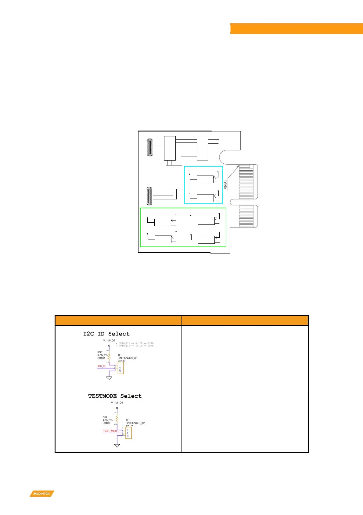
4.2.1 Key Feature and Block Diagram
• Support 4-Lane MIPI CSI Interface and connect with main board through a 36 pin Gold-Finger
• Supports camera module with/without ISP (On-Semiconductor AP1302CSSL00SMGA0-DR)
• 8M pixel camera modules (VF08001 with ON-Semiconductor CMOS image sensor AR0830)
Since there is only one CSI interface from the main board, the D6 DTB can support two camera modules, with ISP and
without ISP, switched by a MIPI multiplexer (TI TS3DV642RUARQ1)
Figure 4-4 Block Diagram of D6 Camera DTB
4.2.2 Configure D6 Camera DTB
Table 4-2 Configure D6 Camera DTB
Schematic Description
(1) Jumper@1-2: ISP I2C address = 0x7A
(2) Jumper@2-3: ISP I2C address = 0x78
(1) Jumper@1-2: Test Mode
(2) Jumper@2-3: Normal
VIN
SCL5/SDA5
V_1V05_D6
V_1V2_D6
V_3V3_D6
EN
V_2V7_D6
V_2V8_D6
BUCK
FP6381
VIN
S0 H
ISP
AP1302
S1
CSI0
34
V_1V8_D6
V_3V3_D6
18
CSI0
CSI1
BUCK
FP6381
EN
I2C_A
MIPI_A
TS3DV642Q1
MUX
I2C_B
MIPI_B
I2C_A
MIPI_A
TS3DV642Q1
MUX
I2C_B
MIPI_B
BUCK
FP6381
LDO
FP6186
VIN
VIN
EN
BM20B(0.8)-34DS-0.4V(51)
17
LDO
FP6186
CSI1
SCL5/SDA5
17
1
SCL0/SDA0
EN
V_3V3_D6
SCL5/SDA5
VIN
EN
V_3V3_D6
CSI
LDO
FP6186
V_3V3_D6
VIN
V_1V0_D6
V_3V3_D6
1
EN
SCL1/SDA1
18
34
 Loading...